What happens when your trillion-dollar AI dreams slam headfirst into a shortage of microscopic glue?
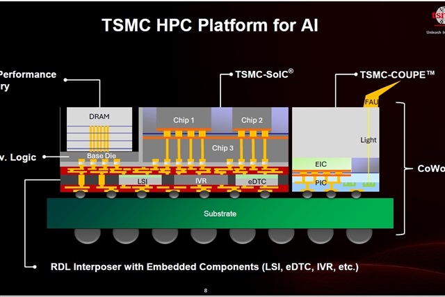
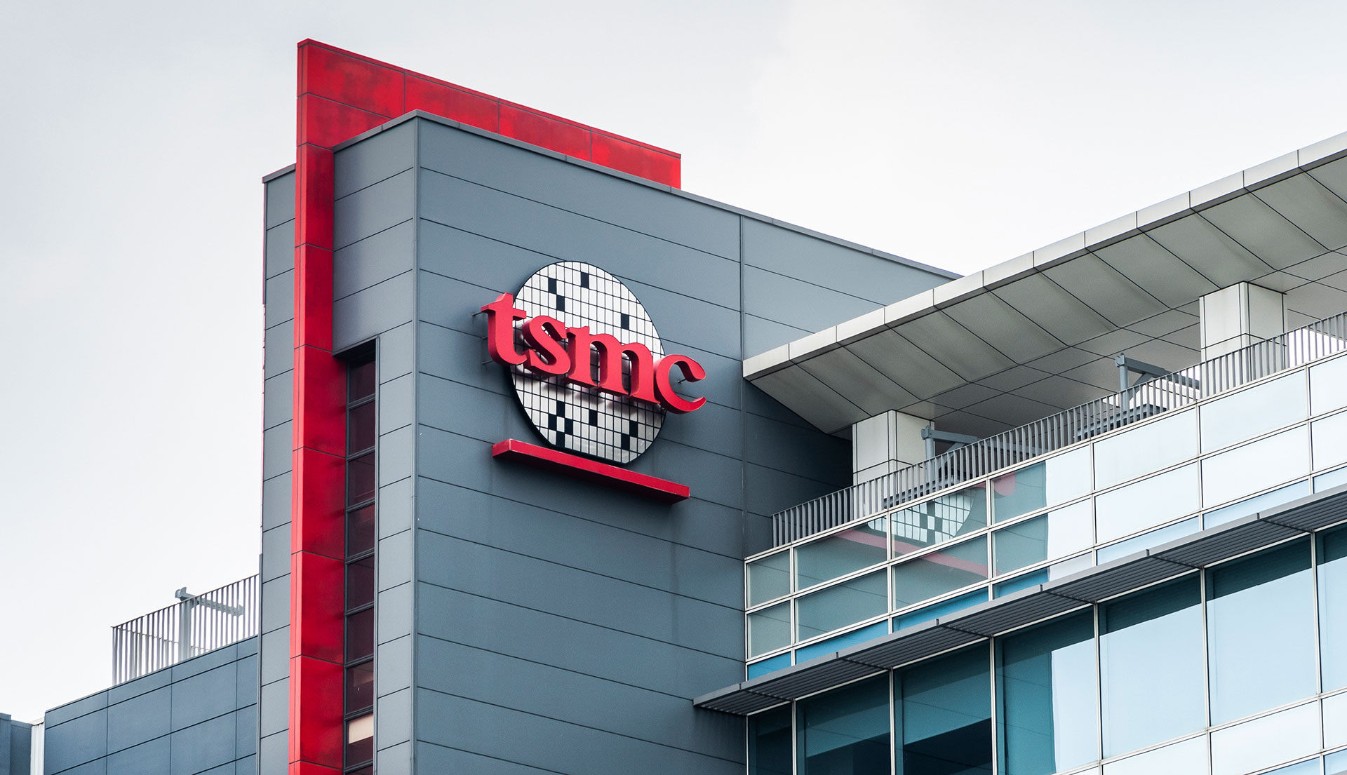
TSMC knows. They’re the invisible giants propping up every Nvidia GPU, every AMD accelerator, every hyperscaler’s server farm—and right now, their advanced packaging lines are creaking under the weight of insatiable demand. It’s not hyperbole: without this tech—stuff like CoWoS, SoIC, WMCM—those behemoth AI chips are just expensive doorstops.
Here’s the thing. Taiwan’s CNA reports TSMC’s going all-in, converting seven older 8-inch wafer fabs in Taiwan for advanced packaging and eyeing two new ones in Arizona. By 2027? Output jumps from 1.3 million wafers to 2 million. That’s not tinkering; that’s a manufacturing moonshot.
“TSMC intends to equip seven fabs with advanced packaging technologies, including CoWoS, WMCM, and SoIC… by 2027, TSMC is expected to reach up to 2 million wafer output, up from 1.3 million.”
But wait—why now? And why does it matter?
Why Is Advanced Packaging AI’s Silent Killer?
Picture this: AI chips have ballooned. Nvidia’s latest Blackwell monsters aren’t single dies anymore; they’re Frankenstein assemblies of multiple chips stitched with ultra-precise interconnects. CoWoS (Chip on Wafer on Substrate) lets you stack ‘em dense, efficient, power-hungry enough for training GPT-6 or whatever beast comes next. Without it, you’re stuck with yesterday’s tech—slower, hotter, thirstier.
Demand? Exploding, mostly from high-performance computing (HPC), aka AI data centers. Mobile gets a slice, sure, but HPC’s the gorilla here. TSMC’s been at 100%+ utilization for months; customers like Apple, AMD, Nvidia are circling competitors like Intel’s EMIB. But Intel? Not scaled for this tsunami.
TSMC’s fix isn’t just more factories—it’s architectural warfare. Retooling 8-inch fabs (older, cheaper) for packaging sidesteps the eye-watering costs of bleeding-edge 3nm lines. Smart. It’s like turning your grandpa’s garage into a rocket assembly plant—efficient, under-the-radar.
And the US push? Arizona’s two new AP facilities hit mass production by 2030. Geopolitics baked in: diversify from Taiwan quake risks, US-China tensions. But 2030 feels distant when Nvidia’s screaming for capacity today.
How Does TSMC Pull This Off Without Melting Down?
Massive investments. We’re talking tens of billions—$65B+ in US fabs alone, per recent chatter, with AP as the crown jewel. Taiwan’s seven fabs get tricked out for CoWoS (HPC king), SoIC (3D stacking wizardry), WMCM (whole-module madness for mobiles).
The why: scale solves everything. AI packages are growing—each gen bigger, more complex. H100 to H200? Packaging bloat. Blackwell? Monstrous. TSMC’s not just building capacity; they’re future-proofing against exponentiating demand.
Look, I’ve seen this movie before. Remember the 2018 crypto boom? GPU shortages crippled miners. TSMC ramped nodes, prices crashed, innovation surged. Parallel here—advanced packaging is the new node war. But bolder prediction: this unlocks hybrid AI architectures we haven’t dreamed of. Think disaggregated chips, shipped globally, assembled locally. TSMC becomes the AI world’s FedEx and UPS.
Critique time. TSMC’s PR spins this as smoothly expansion—bull. Converting fabs risks yield nightmares; Arizona’s unproven (delays already plague their logic fabs). Competitors whisper: Intel’s Foveros, Samsung’s I-Cubelet. If TSMC stumbles, it’s 2025 shortages 2.0.
Still, they’re the undisputed champ. No one’s touching their yield, their ecosystem lock-in.
Is TSMC’s US Gamble Worth the Headache?
Arizona: two AP plants, 2030 production. Noble for supply chain resilience—Trump-era CHIPS Act funneled $6.6B subsidies—but timelines scream caution. TSMC’s Phoenix fabs already slipped; skilled labor’s scarce, costs 4x Taiwan’s.
Yet here’s the insight no one’s yelling: this bifurcates the world. Taiwan fabs feed Asia’s AI frenzy (China gray markets notwithstanding). US gets “secure” supply for DoD, hyperscalers. Architectural shift? Absolutely. Expect split silicon: export-controlled AP for West, full-throttle in Taiwan.
By 2030, 30-40% of TSMC’s AP could be stateside. Game-changer if China tensions spike.
Why Developers — and You — Should Care
Not just suits. If you’re building LLMs, training agents, this means cheaper, faster inference rigs. No more bidding wars for H100s. Stock up on B200s without premium pain.
Broader: AI’s energy hog status? Better packaging = denser compute = less sprawl. TSMC’s ramp could shave gigawatts off data center thirst.
Skeptical take: Hype alert. 2M wafers sound huge, but Blackwell’s a hog—demand might lap supply again. TSMC’s admitting defeat on current constraints; that’s no victory lap.
Punchy truth.
TSMC’s betting the farm. If they nail it, AI accelerates. Botch it? Cue the chaos.
🧬 Related Insights
- Read more: AD Technology’s Samsung Switch: 2nm CPUs Targeting KRW1T Revenue Windfall
- Read more: PCIe 8.0: The Speed Doubler That Might Just Trip Over Its Own Cables
Frequently Asked Questions
What is TSMC advanced packaging and why is it crucial for AI?
It’s tech like CoWoS that stacks multiple chips into powerful modules. Crucial because AI chips like Nvidia’s need it for speed, efficiency—without it, no massive models.
When will TSMC’s new packaging capacity come online?
Taiwan fabs ramp through 2027 (2M wafers); Arizona by 2030. Bottlenecks ease mid-decade.
Will TSMC’s investments fix AI chip shortages?
Likely yes for packaging, but node capacity lags. Expect relief, not miracles.