The real story behind Siemens EDA’s latest pact with TSMC isn’t about a press release; it’s about the sanity of chip designers navigating a universe of ever-increasing complexity. Forget the slick marketing; this collaboration is a pragmatic push to make AI the indispensable co-pilot for engineers tasked with building the silicon brains of tomorrow’s AI accelerators, HPC clusters, and automotive marvels. The stakes are stratospheric, and traditional design methods are buckling under the weight of it all.
The AI Overload: Why Designers Need Help
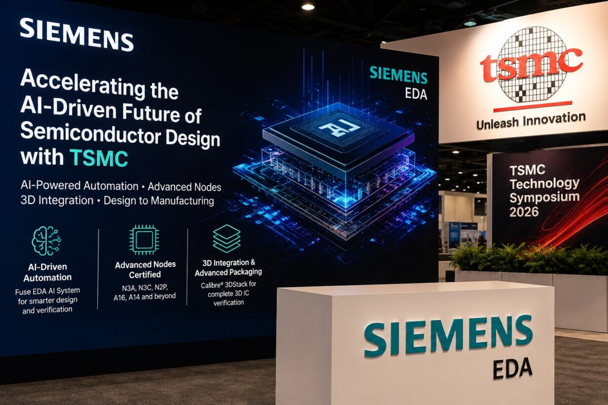
The semiconductor industry’s annual TSMC Technology Symposium used to be a quiet affair for the initiated. Now, it’s a battleground of innovation, and Siemens EDA, a perennial player, is making its AI ambitions known. The core announcement: an intensified collaboration with TSMC aimed squarely at injecting AI-powered automation across the entire semiconductor design workflow. We’re talking about automated Design Rule Check fixing — a task that has historically consumed vast swathes of engineer time — and AI-assisted physical verification. Siemens is even touting its Fuse EDA AI System as the engine behind intelligent design optimization.
This isn’t some futuristic pipe dream. The brutal reality is that chip complexity is exploding. AI chips, designed for lightning-fast computation, demand more sophisticated architectures. High-performance computing processors are pushing boundaries. Automotive processors need to be utterly reliable. And the rise of chiplet-based architectures, where smaller, specialized dies are assembled into a larger system, adds layers of integration challenges. Designers are wrestling with multi-die systems, mind-boggling 3D packaging, data throughput that would make a supercomputer blush, and power delivery nightmares. It’s a juggling act where dropping even one ball means billions in lost investment and delayed product launches.
“AI-enabled EDA tools are becoming critical to reducing development cycles and improving productivity.”
The integration of Siemens’ AI tech into established production-proven tools like Calibre and Aprisa is significant. This isn’t just theory; it’s about making the tools engineers use every day smarter, faster, and less prone to human error. TSMC is reportedly working with Siemens to streamline multi-step automation for physical verification, a process that’s often a bottleneck. The promise? Faster access to critical design insights and guided recommendations. Think less staring blankly at error logs and more directed problem-solving.
Staying Ahead of the Nanometer Curve
The race to the next process node is relentless, and Siemens EDA is ensuring its tools are ready. The company is reporting certifications for its EDA tools across TSMC’s bleeding-edge nodes: N3A, N3C, N2P, A16, and A14. For any semiconductor company sinking billions into developing on these advanced processes, validated design flows are non-negotiable. These certifications act as a green light, allowing chipmakers to begin development with the confidence that their designs won’t hit a wall later down the line. It’s a crucial, if unglamorous, part of the ecosystem that keeps the silicon engine running.
The 3D Puzzle: Packaging Gets Smarter
Advanced packaging isn’t just a buzzword anymore; it’s fundamental to enabling the next generation of AI systems. TSMC’s 3DFabric and CoWoS packaging technologies are at the forefront, and Siemens is clearly playing catch-up here. Their Calibre 3DStack platform is being positioned to handle the intricacies of 3D integration, offering capabilities for interface checking, connectivity verification, and inter-chiplet Design Rule Check (DRC) validation. The ability to analyze current density and antenna effects in these 3D stacked environments is paramount, especially as AI processors increasingly embrace heterogeneous integration—mashing together logic, memory, photonics, and specialized accelerators within a single package. It’s like building a skyscraper where each floor has a different purpose, and you need to ensure every pipe and wire connects perfectly.
The EDA Arms Race
Industry observers have been noting the increasingly fierce competition among the top EDA vendors: Siemens, Synopsys, and Cadence. While all three are undoubtedly expanding their collaborations with TSMC, Siemens appears to be carving out a niche by emphasizing what it calls “agentic AI orchestration” and a deep integration from design to manufacturing. Their strategy seems laser-focused on automating complex workflows that have historically demanded extensive, manual engineering intervention. This is where the real productivity gains will be found.
The timing of these announcements couldn’t be more critical. TSMC’s roadmap is packed with sub-2nm technologies, backside power delivery innovations, advanced automotive nodes, and even co-packaged optics. Each of these represents a fresh set of design and verification hurdles. Companies are under immense pressure to slash design turnaround times while simultaneously hitting ambitious power, performance, and reliability targets. In this environment, AI-assisted automation isn’t just a nice-to-have; it’s rapidly becoming the only viable path to sustaining any semblance of productivity improvement at these advanced nodes.
Siemens’ continued participation in TSMC’s Open Innovation Platform (OIP) is a proof to the value of these deep, long-standing partnerships. The OIP model fosters tight integration between foundry technologies and EDA tool providers, ensuring that design flows are not only optimized but also enabled early on. This synergistic approach is what allows companies like Siemens to remain intrinsically linked to TSMC’s technology evolution, giving them a significant advantage.
The broader semiconductor market dynamics provide the backdrop for these discussions. The insatiable demand for AI capabilities is fueling unprecedented growth, particularly in the high-performance computing infrastructure sector. Advanced packaging, power delivery innovations, and chiplet architectures are no longer fringe concepts; they’re central to competitive differentiation. As these challenges mount, EDA vendors are evolving, shifting from mere software suppliers to becoming strategic enablers of complex silicon innovation. The question is no longer if AI will transform chip design, but how quickly it can realistically be deployed to solve the most pressing problems facing engineers today.
🧬 Related Insights
- Read more: Amazon’s Jassy: Trainium and Graviton Now Gunning for NVIDIA’s Throne
- Read more: ULTRARAM’s AI Synapse Gambit: Hype or Hardware Holy Grail?
Frequently Asked Questions
What does Siemens EDA do? Siemens EDA provides electronic design automation (EDA) software and services that help engineers design, verify, and manufacture complex integrated circuits (ICs) and electronic systems.
How is AI being used in chip design with TSMC and Siemens? Siemens EDA is integrating AI into its tools to automate tasks like design rule checking, physical verification, and design optimization, aiming to speed up development cycles and improve productivity for chips designed on TSMC’s advanced process technologies.
What is advanced packaging? Advanced packaging refers to sophisticated techniques for assembling semiconductor dies (chips) into a single package, allowing for greater integration, performance, and smaller form factors compared to traditional single-chip packaging. This is crucial for complex systems like AI accelerators.