Three hundred thousand. That’s roughly how many transistors TSMC crams into a square millimeter on its leading-edge nodes. For decades, this relentless shrinking — Moore’s Law in its glorious, silicon-fueled prime — was the engine of progress. Faster chips, lower power, cheaper everything. But here’s the kicker: we’re bumping into the physics and economics of it all. Below 3 nanometers, squeezing more transistors isn’t just harder; it’s bordering on the impossible (or at least, prohibitively expensive). So, what happens when the engine sputters? The industry doesn’t stop; it pivots.
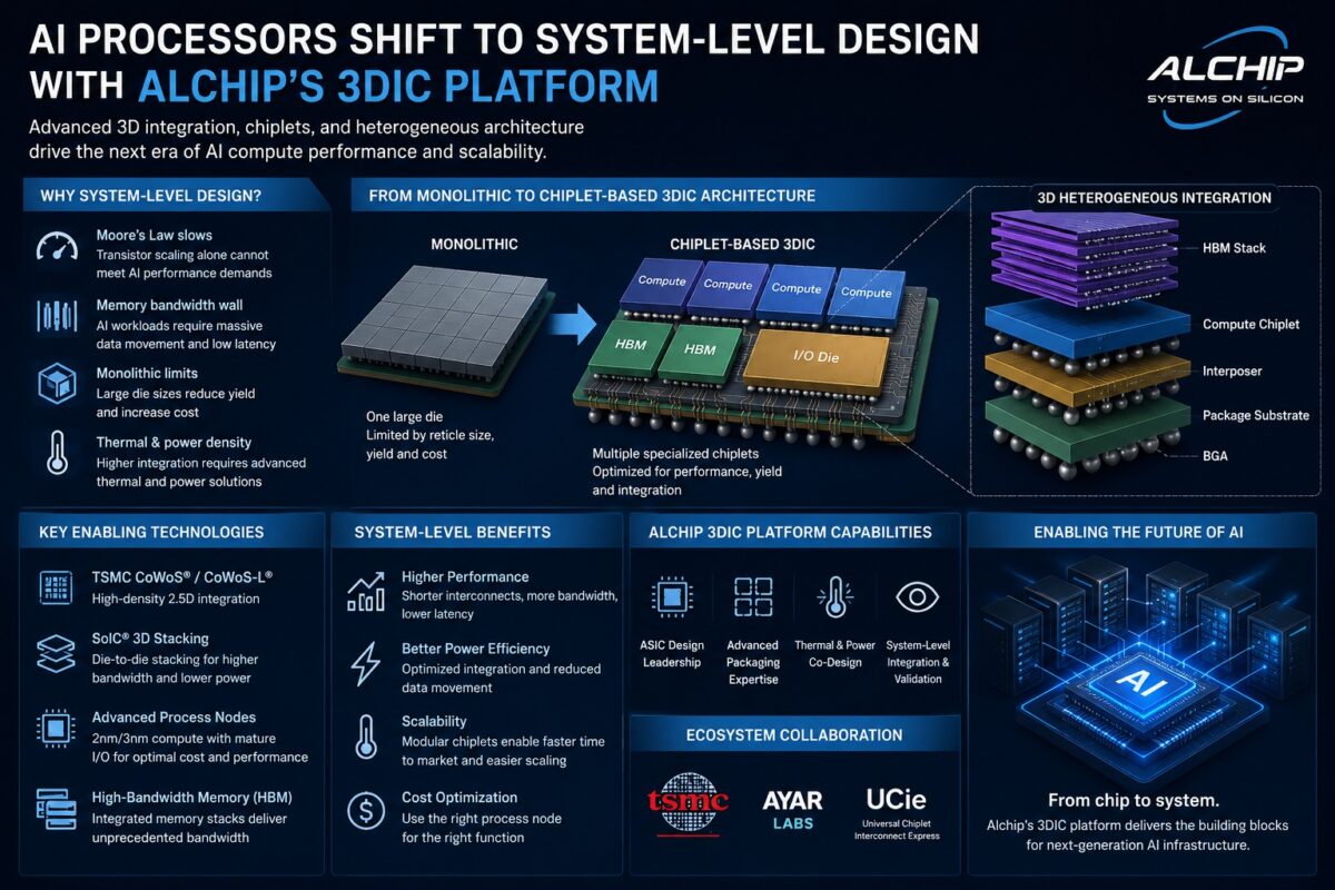
And that pivot? It’s happening vertically, horizontally, and in every conceivable direction around the core silicon. We’re talking about advanced packaging, chiplets, and heterogeneous integration. Think of it like this: instead of building one skyscraper that’s impossibly tall and prone to toppling, we’re building a campus of specialized, interconnected buildings. Each building is optimized for its purpose – one for colossal computation (your AI accelerator), another for lightning-fast memory, maybe even a tiny, dedicated one for optical communication. The glue holding this campus together? That’s the advanced packaging. This is the fundamental platform shift everyone’s whispering about, and the recent announcement that imec IC-Link is joining TSMC’s 3DFabric Alliance is a deafening roar that makes it official.
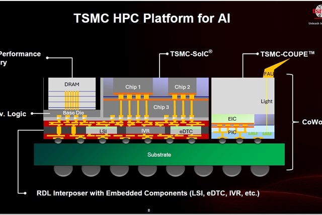
Why should you care? Because this isn’t just about making slightly faster chips for your phone. This is about unlocking the next generation of AI, high-performance computing (HPC), and a dizzying array of other tech that’s going to reshape our world. For so long, the bottleneck wasn’t just the compute power on a single piece of silicon, but the agonizing slowness of data trying to get to that compute, the heat it generated, and the sheer energy it consumed. Advanced packaging technologies like TSMC’s CoWoS (Chip on Wafer on Substrate) and SoIC (System on Integrated Chip) are the superhighways, the hyperloops, the warp drives that solve these inter-chip communication nightmares.
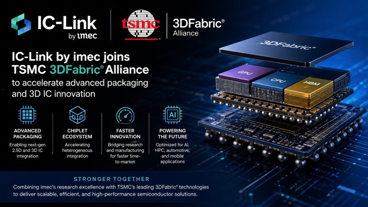
This partnership is incredibly significant because it bridges a chasm. Imec, based in Europe, is a powerhouse of semiconductor R&D. They’ve got the brains, the blueprints, and a deep understanding of everything from silicon photonics to the nitty-gritty of system scaling. TSMC, on the other hand, is the undisputed king of manufacturing, the foundry that turns those blueprints into reality at an unimaginable scale. By having IC-Link — imec’s commercialization arm — join the 3DFabric Alliance, it means that the cutting-edge research happening in imec’s labs can now be directly plugged into TSMC’s massive production ecosystem. It dramatically shortens the journey from a mind-blowing idea to a product that millions can use.
When Packaging Becomes the Architecture
Here’s a seismic insight: packaging is no longer an afterthought. It’s not just the black plastic thingy your CPU sits in. In the age of chiplets, the package is part of the architecture. You can’t just design your chips in a vacuum and then slap them into a box. You have to design the chips and the box together, thinking about heat, power delivery, and how those little bridges between chips will function. This alliance fosters exactly that kind of co-optimization. It’s like an orchestra conductor bringing together the string section, the brass, and the percussion, ensuring they all play in perfect harmony from the very first rehearsal, not just during the concert. This collaboration enables designers to bring complex, multi-die systems to market faster and with fewer headaches.
And for AI and HPC, this is nothing short of a revolution. Think about training those gargantuan AI models that power everything from chatbots to self-driving cars. They guzzle data. They need memory bandwidth that makes traditional systems weep. They demand ultra-low latency connections between processing cores and memory. Traditional packaging just can’t cut it. But with technologies like TSMC’s CoWoS and SoIC, we’re seeing the integration of high-density, die-to-die interconnects and even vertically stacked memory. This isn’t just an incremental improvement; it’s a leap that dramatically boosts bandwidth and slashes power consumption per bit. It’s the secret sauce behind many of the competitive AI accelerators you’re hearing about.
Through the alliance, IC-Link customers gain earlier access to TSMC’s advanced packaging flows and validated ecosystem infrastructure.
This means that startups, especially those in Europe, who might not have the colossal capital to build their own fabrication plants or advanced packaging facilities, can now use TSMC’s world-class infrastructure through imec. It lowers the risk, accelerates the path from a promising prototype to mass production, and democratizes access to the very technologies that are defining the future of computing. It’s a strategic win for Europe, positioning imec not just as a research hub but as a vital gateway into the global semiconductor manufacturing landscape.
What’s Next for Chip Design?
The industry is rapidly moving toward modular semiconductor design. We’re seeing the emergence of standardized chiplet interfaces, allowing companies to mix and match components from different vendors, fostering an ecosystem of innovation similar to how software developers build applications using various APIs and libraries. This modularity reduces development time and cost, as designers can reuse proven chiplets instead of designing every single piece of silicon from scratch. It’s a fundamental paradigm shift that’s going to unleash a wave of new semiconductor products and capabilities.
This imec-TSMC alliance isn’t just a partnership; it’s a declaration of intent. It signals that the era of solely relying on transistor shrinking is over, and we’re entering a new, incredibly exciting phase defined by intelligent integration and system-level optimization. The future of silicon is no longer confined to a single, monolithic die. It’s a vibrant, interconnected ecosystem, and imec and TSMC are building the ultimate bridge for it.
🧬 Related Insights
- Read more: Meta & UC San Diego Unveil TLX Compiler: Boosting GPU ML Production
- Read more: Truck-Sized AI Data Centers: GPUs Delivered in Months, Not Years
Frequently Asked Questions
What does imec IC-Link do? imec IC-Link acts as a bridge between advanced semiconductor research conducted at imec and industrial manufacturing. It helps commercialize new technologies like advanced packaging and heterogeneous integration developed in research labs, connecting them to production partners like TSMC.
Will this alliance make my AI applications faster? Yes, indirectly. By enabling more advanced chiplet architectures and optimized packaging, this collaboration allows for the creation of more powerful AI accelerators and HPC systems that can process data faster, with lower latency, and higher energy efficiency, ultimately benefiting AI applications.
Is this the end of Moore’s Law? While traditional transistor scaling under Moore’s Law is slowing down due to physical and economic limits, the spirit of innovation is alive and well. This alliance signifies a shift towards ‘More than Moore’ – focusing on system-level scaling through advanced packaging, chiplets, and heterogeneous integration to continue driving performance gains.