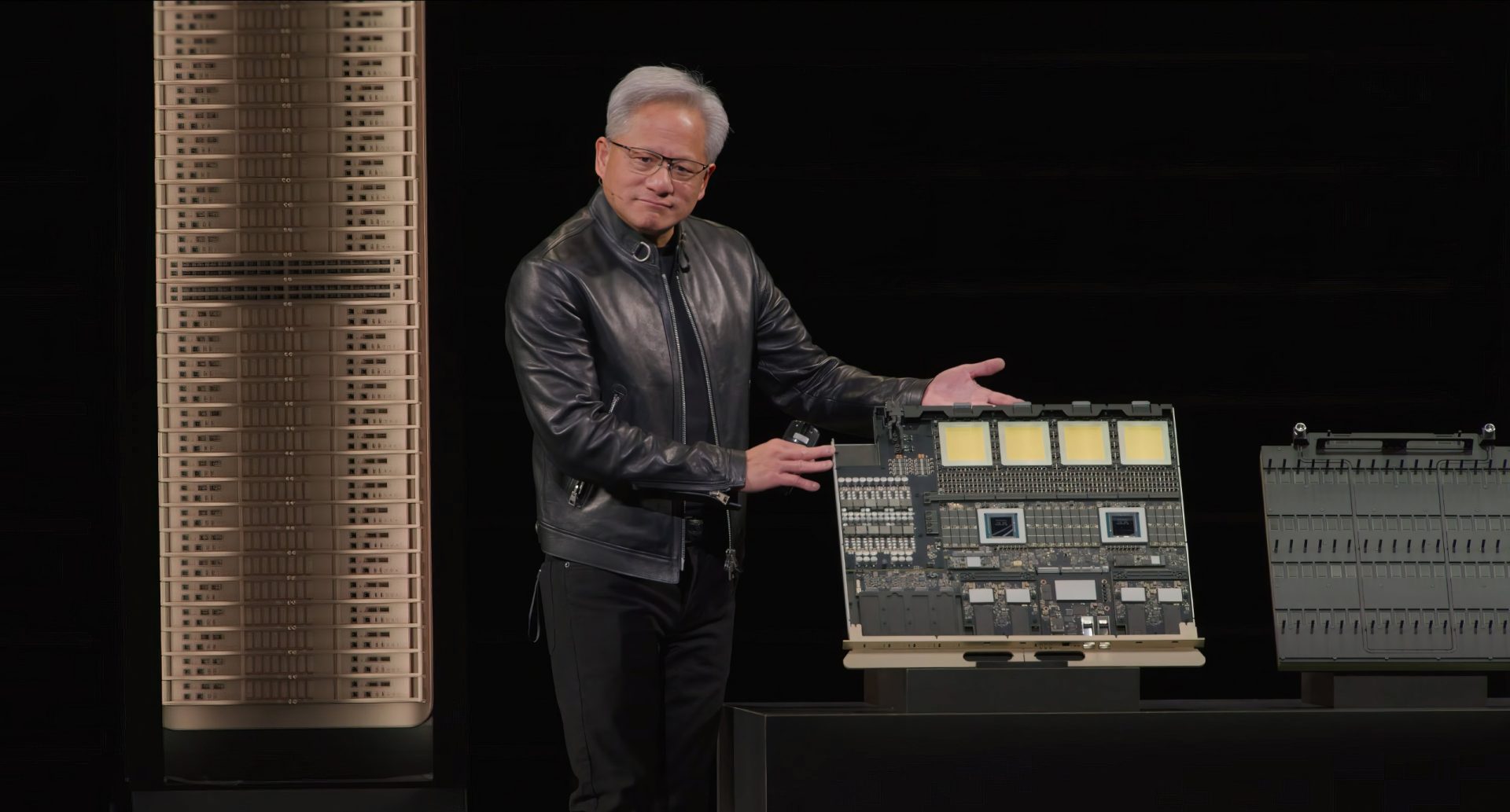
Nvidia’s Rubin Ultra GPU will demand 1TB of HBM per chip by 2027 — a staggering 16x leap from the H100’s 80GB baseline.
And that’s just Nvidia. This isn’t hype; it’s raw market math, with AI accelerators gobbling HBM bits at rates that make DRAM fabs sweat.
HBM — High Bandwidth Memory — sits at the heart of this frenzy. It’s the gold standard for AI training and inference, blending massive bandwidth with decent capacity via those signature stacked dies and ultra-wide buses. Forget DDR5’s penny-pinching density; HBM trades cost for speed where it counts most.
But here’s the kicker. As models balloon — think trillions of parameters — the old memory wall looms. HBM’s scaling it back, one TSV at a time.
What Makes HBM Tick (And So Damn Expensive)?
Stack eight, twelve, even sixteen DRAM layers on a logic base die. Punch through-silicon vias (TSVs) for signals and power. Wire over 1,000 connections to the GPU’s edge — the precious ‘shoreline’ real estate.
This isn’t plug-and-play. SK Hynix’s HBM3 die? Just 0.16 Gb/mm² density — 85% less packed than their DDR4 cousin at 0.296 Gb/mm². Those TSVs eat space, and stacking demands exotic packaging like TSMC’s CoWoS interposer.
“HBM combines vertically stacked DRAM chips with ultra-wide data paths and has the optimal balance of bandwidth, density, and energy consumption for AI workloads.”
Spot on. That’s why every top AI chip — Nvidia’s Blackwell, AMD’s MI300, Google’s TPUs — bolts HBM stacks right to the silicon die. No interposer? You’re toast on bandwidth.
Shoreline scarcity bites hardest. GPUs reserve two edges for I/O; HBM hugs the other two. Pack more? You beachfront expand — widen the SOC edge, add repeaters, or hybridize with LPDDR.
My take? It’s brilliant engineering, but vendors are hitting limits. Enter HBM4’s game-changer: custom base dies.
HBM4’s Custom Base Die: Nvidia, OpenAI, AMD All In
Custom logic base dies for HBM4 aren’t tweaks; they’re a paradigm shift. Ditch generic buffers — tailor the bottom layer for specific accelerators.
Nvidia’s whispering about it for Rubin. OpenAI’s custom silicon? HBM4 stacks with bespoke bases to offload KV cache, slash latency. AMD’s sniffing around too, per supply chain chatter.
This slices power draw, boosts yields. But it locks suppliers tighter to hyperscalers. SK Hynix leads HBM3E shipments now (70%+ share), yet Samsung lags qualification. Micron plays catch-up.
Unique insight: Echoes the 2010s GDDR5 pivot. Nvidia force-fed memory makers HBM, mirroring how GPUs birthed GDDR. Except now, AI’s trillion-dollar stakes mean custom dies could sideline pure-plays — think Samsung’s MR-MUF packaging edge fading if OpenAI fabs its own.
The Shoreline Squeeze: Beachfront Tricks and Offloads
Shoreline — that SOC perimeter for HBM — caps capacity. Double it? Vertical stacks help, but physics rebels. Solution: expand the beach.
Wide buses, high-rank configs (12-HBM stacks). Repeaters bridge longer traces. Compute-under-memory buries logic beneath stacks. Even SRAM tags for faster lookups.
Disaggregated prefill/decode? Offload to NVLink-pooled memory pools. KVCache to HBM edges. It’s all in play, per roadmaps.
But energy? HBM guzzles 30-40% of a GPU’s power envelope. Custom dies + process shrinks (HBM4 at 1β node?) promise relief.
Supply Chain Wildcard: Samsung’s HBM Fight — And China’s Shadow
Samsung’s in the hot seat. Late to HBM3E qual, yet plotting HBM4 with custom dies and domestic China production ramps.
Bit demand? Explosive. Nvidia owns 2027’s lion share, Rubin Ultra at 1TB. Broadcom’s TPUs, OpenAI/SoftBank ASICs pile on.
China’s push? SMIC fabs, CXMT DRAM — but TSV tech lags. Geopolitics adds tariffs, export curbs. US CHIPS Act funnels billions to SK Hynix, Micron.
Samsung’s viability? Dicey. If custom dies proliferate, they risk becoming a me-too supplier. Prediction: By 2028, HBM bit growth flatlines as CXL memory pools + on-package SRAM steal share. One reversal the original misses: compute-in-memory flips the script, embedding logic in DRAM stacks.
Roadmap glance:
-
HBM3E: 9.2 GT/s, 24/36GB stacks. Shipping now.
-
HBM4: 12+ layers, custom bases, 1.2+ TB/s bandwidth. 2026 samples.
Why Does HBM Matter for AI Roadmaps?
Architectures ditching HBM flop. We’ve clocked it: DDR-only chips lag 3-5x on bandwidth-starved inference.
Nvidia’s roadmap screams HBM fidelity — Blackwell 288GB, Rubin 400GB+, Ultra 1TB. AMD matches. Custom ASICs? HBM or bust.
HBM upends DRAM economics. Prices? 5-10x DDR5 premiums stick, demand be damned.
Skeptical spin check: Vendor roadmaps gloss supply crunches. Reality? TSV conversion bottlenecks persist; HBM’s <10% of DRAM capacity today.
Is Samsung Doomed in the HBM Race?
Not yet. Shoreline expansions, LPDDR hybrids give breathing room. But custom dies favor incumbents cozy with TSMC.
China domestic? Risky bet amid bans. SK Hynix’s pole position holds through 2027.
Bold call: HBM peaks mid-decade, then hybrids (HBM + CXL) dominate exascale AI.
🧬 Related Insights
- Read more: This Self-Healing Chip Laughs at Jupiter’s Radiation Onslaught
- Read more: Memory Chip Shortage: AI’s Feast Means Your Famine for Years
Frequently Asked Questions
What is HBM memory used for?
HBM powers AI GPUs and accelerators with stacked DRAM for ultra-high bandwidth — essential for training massive models like GPT.
When does HBM4 launch?
Samples in late 2025, volume 2026 — packing custom base dies for 50%+ bandwidth jumps over HBM3E.
Who supplies HBM for Nvidia GPUs?
SK Hynix dominates (70%+), Samsung catching up, Micron third. Nvidia’s Rubin bets big on all three amid shortages.