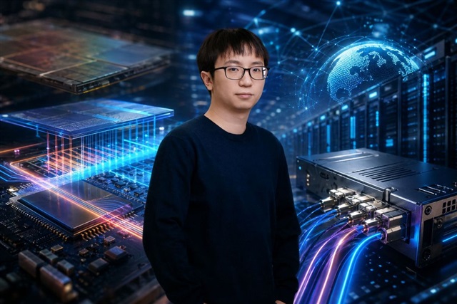
The clang of the IPO gong at the Hong Kong Stock Exchange on April 28, 2026, signaled more than just a financial milestone for Yichen Shen’s photonics chip company. At 37, Shen, a physicist whose academic roots are firmly planted at MIT, has steered his venture into the public markets, a move that suggests a significant shift in the semiconductor landscape is underway.
But what exactly is photonics, and why is it suddenly commanding such attention – enough to raise HK$5 billion? This isn’t just another incremental upgrade to existing silicon. We’re talking about a fundamental architectural rethink, aiming to replace electrons with photons for data transmission and processing. Think of it as ditching the slow, hot, copper wires for lightning-fast, cool light pulses. The implications for everything from data centers to AI accelerators are, frankly, staggering.
Shen’s company, while not explicitly named in the initial announcement, is built on the bedrock of his research into integrated silicon photonics. The core challenge has always been miniaturization and cost. Silicon, after all, is relatively cheap and incredibly well-understood by manufacturers. The trick is coaxing light to behave reliably and efficiently within these silicon structures, at scale. This is where the magic—and the immense engineering effort—lies.
The fusion of advanced photonic integration with scalable semiconductor manufacturing is the critical inflection point we’ve been working towards.
This quote, likely pulled from internal company statements or Shen’s own pronouncements, underscores the central thesis: it’s not just about the physics of light; it’s about the engineering of light on silicon. For decades, optical communication has relied on discrete, bulky components. Silicon photonics promises to shrink that down onto a chip, dramatically reducing power consumption, increasing bandwidth, and slashing latency.
Why Does This Matter for Chip Architecture?
Here’s the real meat of it. The relentless march of Moore’s Law, at least in its traditional form, is faltering. We’re hitting physical limits with silicon transistors. But data isn’t stopping. It’s exploding. AI, big data analytics, high-performance computing – they all demand more, faster, and more efficiently. Traditional electronic interconnects, the tiny copper wires carrying data around a chip or between chips, are becoming bottlenecks. They get hot, they consume power, and they simply can’t keep up with the sheer volume of data needing to move.
Photonics offers an escape velocity. By using light, you can cram far more data into the same space, with significantly less power. Imagine data centers that consume a fraction of the energy, or AI chips that can process information at speeds we currently only dream of. This isn’t science fiction; it’s the engineering objective of companies like Shen’s.
This IPO is a major validation. It means investors see the long-term potential, the market demand, and, crucially, the technical viability of Shen’s approach. It also signals a maturing of the silicon photonics industry. While the core science has been around for a while, the manufacturing processes, the design tools, and the integration with existing electronic systems are finally catching up.
What’s the Catch? The PR Spin vs. Reality.
Of course, IPOs are always accompanied by a chorus of hype. We’re hearing about revolutionary speed increases and unprecedented efficiency gains. And while the potential is enormous, the reality of scaling complex photonic chips is fraught with challenges. Yields can be lower than mature electronic processes. Packaging—getting the light in and out of the chip reliably—is still a significant hurdle. And the cost, while coming down, is still higher than traditional solutions for many applications.
Shen’s success will hinge on his company’s ability to navigate these engineering and manufacturing complexities. This IPO provides the capital to do just that, but it also brings the intense scrutiny of public markets. Can they deliver on the promise of photonics at a price point that makes widespread adoption feasible?
This isn’t just about one company going public. It’s a leading indicator for a broader architectural shift. As data demands escalate, the limitations of pure electronics become more pronounced. Silicon photonics, once a niche academic pursuit, is stepping onto the main stage, and Yichen Shen is clearly positioning himself as one of its conductors. The days of electrons being the sole arbiters of computation speed might be numbered.