Five years early.
That’s the headline, isn’t it? NVIDIA, the company that practically invented ‘fast-forward,’ has decided its Feynman GPUs apparently can’t wait for the future of silicon photonics. Co-Packaged Optics (CPO), the stuff of 2033 roadmaps, is now slated for a 2028 arrival. Because, you know, AI factories are apparently really impatient.
Here’s the deal: CPO is supposed to be the hot new thing. It ditches copper for light, promising zippier connections and less power consumption between accelerators like GPUs. Think of it as upgrading from a garden hose to a fiber optic cable for your data. The whole point is to make these massive AI clusters hum with less latency and more bandwidth. Standard stuff, really, for anyone trying to move petabytes of data at speeds that would melt your old modem.
So, why the rush? The article dangles the carrot of scaling AI firms needing to push data across distances that make a sprint look like an epic journey. We’re talking 10km of optical magic, shifting hundreds of gigabits per second. Copper just can’t keep up without becoming a molten mess. And NVIDIA, being NVIDIA, wants to be the first to the party, naturally.
It’s all part of this OCI-MSA thing, a group of heavy hitters (AMD, Meta, OpenAI, Microsoft – the usual suspects) trying to nail down standards. NVIDIA, always eager to wave its flag, is leading the charge with Feynman. This isn’t just a minor tweak; it’s a strategic acceleration that reshapes the competitive landscape.
Feynman’s Fancy Bits: 3D Stacking and Custom HBM
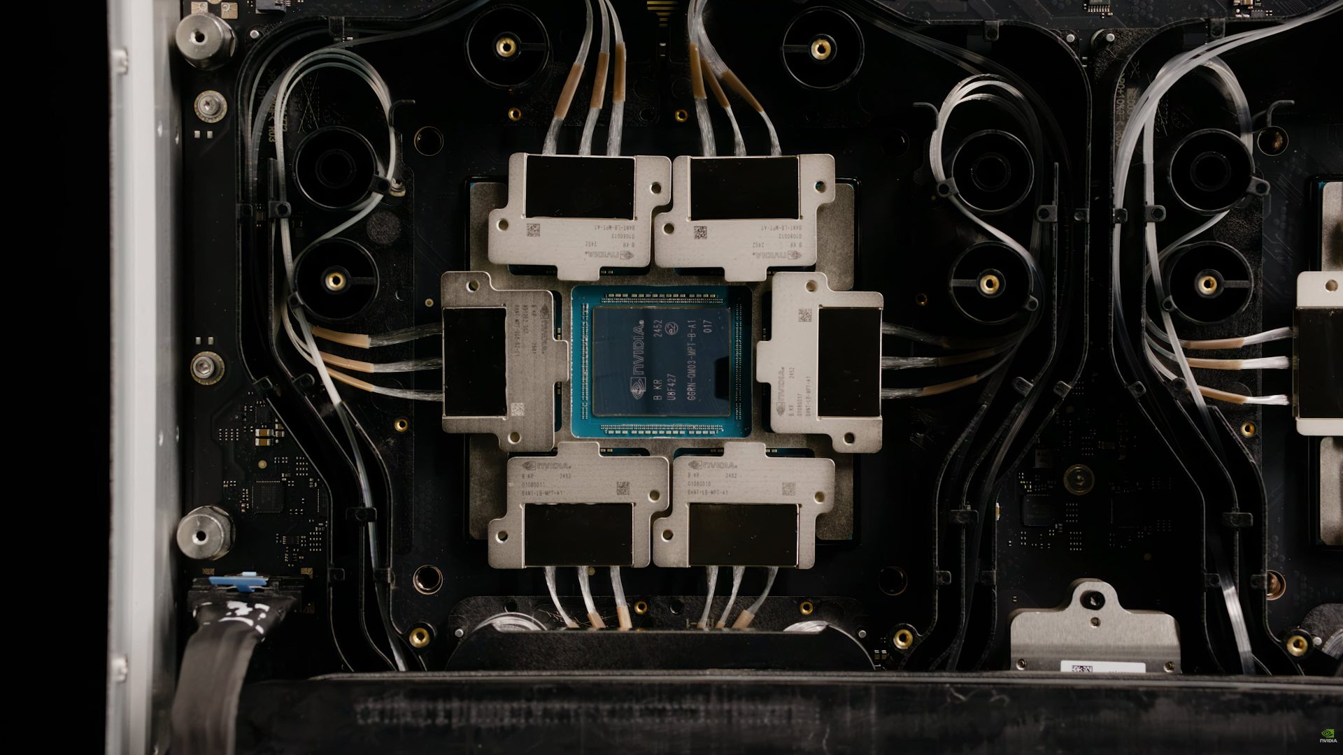
And the surprises don’t stop with CPO. NVIDIA’s Feynman GPUs are also getting the 3D Die Stacking treatment. This means stacking chips on top of each other, a technique that’s been talked about for ages but is apparently finally making its debut with these GPUs. They’re even leaning on Intel’s advanced packaging tech, like EMIB, to get it done. It sounds like a recipe for cramming more power into a smaller, denser package.
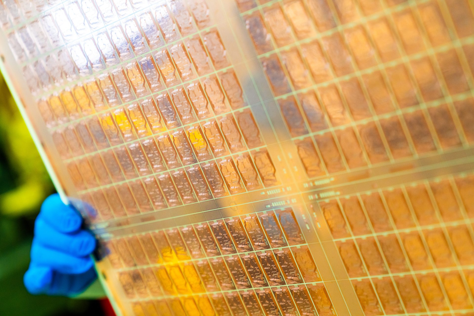
Then there’s the memory. Forget standard HBM. NVIDIA’s Feynman will sport custom HBM. While the article is a bit vague—suggesting it’s a custom or heightened version of HBM4E or even a custom HBM5—the implication is clear: NVIDIA is aiming for something beyond the off-the-shelf offerings. They want their silicon to have a memory advantage that others can’t easily replicate.
Oh, and a new CPU architecture named Rosa. Because naming server CPUs after physicists is apparently the thing to do. It’s named after Rosalyn Sussman Yalow, another Nobel laureate. No details, of course, but given NVIDIA’s track record, expect it to be… more.
And the accompanying bits? BlueField-5, NVLink 8 CPO, Spectrum 7 204T, CX10. A whole ecosystem being prepped for this 2028 rollout. AMD’s reportedly playing catch-up, aiming for a similar 2028 debut with their MI500 GPUs. Competition, as always, is a powerful motivator.
But here’s the real kicker, the thought that keeps nagging: Is this acceleration about genuine technological necessity, or is it about NVIDIA flexing its muscles? Companies don’t typically pull multi-year roadmaps forward unless there’s a compelling, often market-driven, reason. Is the demand for raw AI compute so explosive that waiting even two years for optical interconnects is a bottleneck they must break? Or is this simply NVIDIA ensuring they maintain their formidable lead, forcing competitors to scramble and invest even more heavily in catching up, all while they dictate the pace of innovation?
It feels like a calculated gamble, a power play that shifts the industry’s timeline dramatically. They’ve effectively declared their intent: the future of high-performance computing isn’t just coming; it’s arriving five years early, and NVIDIA is holding the boarding pass.
The OCI-MSA announced the establishment back in March, involving major AI firms such as NVIDIA, Broadcom, AMD, Meta, OpenAI, and Microsoft. NVIDIA, being the largest of the bunch, is bringing out its first Co-Packaged solution with Feynman GPUs in 2028.
NVIDIA Data Center / AI GPU Roadmap
| GPU Codename | Feynman | Rubin (Ultra) | Rubin | Blackwell (Ultra) | Blackwell | Hopper | Ampere | Volta | Pascal |
|---|---|---|---|---|---|---|---|---|---|
| GPU Family | GF200? | GR300? | GR200? | GB300 | GB200/GB100 | GH200/GH100 | GA100 | GV100 | GP100 |
| GPU SKU | F200? | R300? | R200? | B300 | B100/B200 | H100/H200 | A100 | V100 | P100 |
| Process Tech | TSMC A16? | TSMC N2P? | TSMC N3P? | TSMC 4NP | TSMC 4NP | TSMC 5nm | TSMC 7nm | TSMC 12nm | TSMC 16nm |
| CPU | Rosa | Vera | Vera | Grace | Grace | Grace | N/A | N/A | N/A |
| Memory | HBM4e/HBM5? | HBM4 | HBM4 | HBM3e | HBM3e | HBM2e/HBM3/HBM3e | HBM2e | HBM2 | HBM2 |
| Launch | 2028 | 2027 | 2026 | 2025 | 2024 | 2022-2024 | 2020-2022 | 2018 | 2016 |
🧬 Related Insights
- Read more: Arm’s $1T TAM Gambit: A Swiss Identity Crisis?
- Read more: Newegg’s $990 Ryzen 9800X3D Bundle: AMD’s Gaming Beast at Bargain-Basement Blues
Frequently Asked Questions
What is Co-Packaged Optics (CPO)?
CPO integrates optical interconnects directly onto the same package as compute chips like GPUs. This allows data to be transferred using light instead of copper wires, promising higher bandwidth, lower latency, and improved power efficiency for AI and high-performance computing.
When will NVIDIA’s Feynman GPUs with CPO be available?
NVIDIA’s Feynman GPUs, featuring Co-Packaged Optics, are slated for release in 2028, significantly ahead of previous industry projections.