The semiconductor industry is undergoing a fundamental architectural shift. For decades, the path to better chips was straightforward: shrink the transistors, pack more onto a single monolithic die, and increase performance. But as transistor scaling becomes harder and more expensive, the industry is embracing a new paradigm: chiplets, small modular dies assembled together using advanced packaging to create complex systems that would be impractical or impossible to build as a single chip.
Why Monolithic Scaling Is Hitting Limits
A monolithic chip is manufactured as a single piece of silicon. As chips grow larger to accommodate more transistors, yields drop dramatically. Yield, the percentage of functional dies per wafer, decreases exponentially with die area because a single defect anywhere on the die renders the entire chip non-functional.
Consider a wafer with a defect density of 0.1 defects per square centimeter. A small die of 100 square millimeters might achieve 90% yield. A large die of 800 square millimeters, the size of a modern GPU or server processor, might yield only 45%. This means over half of the large dies on every wafer are discarded, driving up the effective cost per working chip.
The economic challenge compounds at advanced process nodes. Manufacturing at 3nm costs roughly twice as much per wafer as 5nm, which itself costs significantly more than 7nm. Not every part of a chip benefits equally from being on the latest node. Cache memory, I/O circuits, and analog components often perform adequately on older, cheaper nodes. Building everything on 3nm wastes money on components that do not need it.
The Chiplet Solution
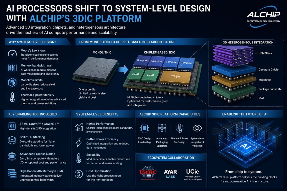
Chiplets address these problems by decomposing a large monolithic chip into smaller, modular dies that are manufactured separately and then assembled together in a package. Each chiplet can be built on the process node most appropriate for its function: high-performance compute chiplets on 3nm, memory controllers on 5nm, and I/O chiplets on a mature 12nm or 16nm process.
This approach offers several advantages. Smaller dies have dramatically better yields, reducing waste and cost. Chiplets can be mixed and matched to create product variants without designing entirely new chips. A server processor might use eight compute chiplets for a high-end product and four for a mid-range product, sharing the same I/O and memory controller chiplets. This modularity reduces design costs and time-to-market.
AMD was the pioneer of chiplet architecture in high-volume products. Its EPYC server processors, starting with the Rome generation in 2019, use multiple compute chiplets (CCDs) connected to a central I/O die (IOD). This design allowed AMD to compete with Intel's monolithic server processors by combining affordable 7nm compute chiplets with a 14nm I/O die, achieving both high performance and competitive pricing.
Advanced Packaging Technologies
Chiplets are only useful if they can be connected with enough bandwidth and low enough latency to function as a coherent system. Advanced packaging technologies provide this connectivity, and they are rapidly becoming as important as transistor scaling in determining chip performance.
2.5D Packaging with Interposers
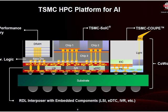
In 2.5D packaging, multiple dies are placed side by side on a silicon interposer, a thin piece of silicon containing a dense network of wires (through-silicon vias, or TSVs) that connect the dies. The interposer provides much higher interconnect density and bandwidth than a traditional organic package substrate.
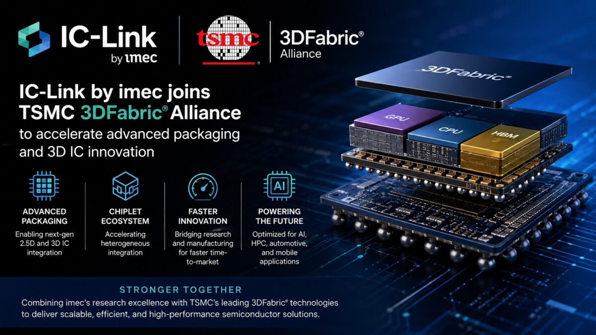
TSMC's Chip-on-Wafer-on-Substrate (CoWoS) is the most widely used 2.5D packaging technology. NVIDIA's H100 GPU uses CoWoS to connect the GPU die with HBM memory stacks, and virtually every advanced AI accelerator uses some form of 2.5D packaging for HBM integration. Demand for CoWoS capacity has been a significant bottleneck in AI chip production, with TSMC aggressively expanding its CoWoS facilities.
3D Stacking
Three-dimensional stacking places dies directly on top of each other, connected by TSVs running vertically through the silicon. This approach offers the highest possible interconnect density and bandwidth because the connections are extremely short. HBM (High Bandwidth Memory) is the most successful commercial example of 3D stacking, with multiple DRAM dies stacked vertically and connected to a logic die at the base.
AMD's 3D V-Cache technology applies 3D stacking to processor cache. The Ryzen 7 5800X3D, launched in 2022, stacked an additional 64MB of SRAM cache on top of the existing CCD, tripling the available L3 cache without redesigning the processor. The additional cache dramatically improved gaming performance, demonstrating that 3D stacking can deliver meaningful benefits even for consumer products.
TSMC's SoIC (System-on-Integrated-Chips) technology enables more aggressive 3D integration, including chip-on-wafer stacking where known-good dies are bonded directly to a wafer at extremely fine pitch. This technology is expected to enable tighter integration of logic-on-logic stacking in future processor generations.
Hybrid Bonding
Traditional chip stacking uses micro-bumps, tiny solder balls that connect pads between stacked dies. Hybrid bonding eliminates these bumps by directly fusing copper pads and oxide surfaces between dies, allowing much finer pitch connections (less than 1 micrometer versus 25+ micrometers for micro-bumps). This dramatically increases the number of connections per unit area, enabling bandwidth-hungry applications like logic-on-logic stacking.
Intel's Foveros technology uses hybrid bonding for 3D integration. The company's Meteor Lake processors, launched in late 2023, use Foveros to stack a compute tile on top of a base tile, with the base tile providing connectivity to I/O and other chiplets. This was one of the first high-volume consumer products to use 3D hybrid bonding.
Industry Standards: UCIe
One of the challenges with chiplet architectures is interoperability. If every company uses proprietary interfaces between chiplets, the modularity benefits are limited. The Universal Chiplet Interconnect Express (UCIe) standard, published in 2022, aims to solve this by defining a common die-to-die interface.
UCIe specifies electrical signaling, protocol layers, and physical dimensions for chiplet interconnects. It supports both standard-package connections (for side-by-side chiplets on an organic substrate) and advanced-package connections (for chiplets on a silicon interposer or bridge). Major companies including Intel, AMD, ARM, TSMC, Samsung, and Google have backed the standard.
The vision of UCIe is a future where chiplets from different vendors can be mixed and matched like LEGO blocks, with a processor chiplet from one company connected to an accelerator chiplet from another and a memory chiplet from a third. This vision is still years from realization, but the standard lays the groundwork for a more modular and flexible chip design ecosystem.
The Economics of Chiplets
The economic case for chiplets becomes more compelling as process nodes become more expensive. At the 3nm node, a full mask set costs approximately $25 million, and a complete chip design can cost $500 million or more in engineering time and IP licensing. Chiplet architectures allow companies to amortize these costs across more products by reusing chiplets in different configurations.
However, chiplets also introduce costs. Advanced packaging is expensive, with CoWoS and 3D stacking adding significantly to per-unit costs. Testing becomes more complex because individual chiplets must be validated before assembly, and the assembled package must be tested again. Thermal management is more challenging when heat-generating dies are placed close together or stacked vertically.
Despite these challenges, the industry consensus is clear: chiplets and advanced packaging are the future. AMD, Intel, Apple, NVIDIA, and every major chip designer have adopted or are adopting chiplet architectures. The companies that master advanced packaging will have a decisive advantage in delivering the performance, efficiency, and cost targets that next-generation applications demand.
Looking Ahead
The convergence of chiplet architecture and advanced packaging is enabling a new class of semiconductor products that blur the line between a chip and a system. AMD's MI300X combines GPU compute chiplets, CPU chiplets, and HBM memory in a single package. NVIDIA's GB200 Grace Blackwell Superchip integrates CPUs and GPUs with high-bandwidth interconnects. Apple's M-series Ultra chips fuse two dies using a silicon interposer to double performance.
Future developments will push integration further. Optical interconnects between chiplets could enable higher bandwidth over longer distances. Photonic chiplets integrated into the package could connect directly to fiber optic networks. And as UCIe matures, the possibility of a standardized chiplet marketplace, where companies can buy and integrate best-in-class chiplets rather than designing everything in-house, could democratize access to advanced silicon capabilities.