The hum of servers in a hyperscale data center is the sound of progress, but increasingly, it’s also the sound of a bottleneck. As artificial intelligence systems scale towards the insatiable demands of the AI era, the chips themselves are getting smaller, smarter, and more numerous – thanks to chiplets. The problem? They’re struggling to keep pace with the sheer volume of data they need to exchange, a fundamental limitation Syenta aims to obliterate.
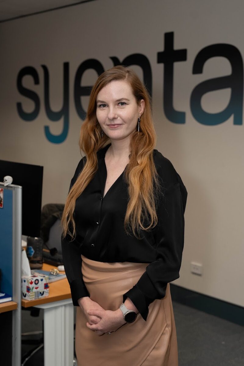
Dr. Jekaterina Viktorova, Syenta’s CEO and Co-Founder, is at the helm of this ambitious mission. With a background steeped in electrochemistry and advanced manufacturing, she’s the architect behind the company’s Localized Electrochemical Manufacturing (LEM) technology. This isn’t just another incremental improvement; Syenta claims LEM can enable ultra-high-resolution copper interconnects, the digital superhighways for next-generation advanced packaging, directly addressing what’s becoming known as the AI era’s memory bandwidth bottleneck.
Syenta’s core pitch is elegantly simple: the future of AI and high-performance computing (HPC) lies in increasingly sophisticated chiplet-based architectures. Think of it as a Lego set for processors, where specialized compute, memory, and I/O units are assembled into a single package. The issue, however, is that current interconnect technologies, the tiny bridges connecting these individual pieces, are simply not dense enough or fast enough to handle the torrent of data required. This is where Syenta steps in.
Their LEM approach isn’t about building entirely new fabs or process lines from scratch — a costly and time-consuming endeavor. Instead, it’s designed to integrate with existing semiconductor manufacturing infrastructure. This is a critical differentiator. Many advanced packaging solutions require massive capital investment and extended development cycles. Syenta’s path suggests a faster, more accessible route to higher-density interconnects, promising to unlock greater performance and scalability without the daunting barriers of entry.
“We’ve developed a proprietary manufacturing approach, Localized Electrochemical Manufacturing (LEM), that enables finer-pitch, high-density chip-to-chip connections using existing fabrication infrastructure,” Viktorova explains. “Our goal is to unlock higher performance and scalability for AI and high-performance computing systems while making advanced packaging more accessible and manufacturable at scale.”
The Interconnect Crunch
What exactly keeps the architects of AI’s future up at night? It’s the palpable reality of hitting physical limits. As hyperscale data centers churn through ever-larger models, the demand for bandwidth and low latency between interconnected chips becomes paramount. Current chiplet integration methods are straining under this pressure. The bandwidth available per chiplet is becoming a choke point, directly impacting everything from training times for massive AI models to the overall power efficiency of these complex systems.
Beyond performance, there’s the gnawing concern over supply chain resilience. The advanced packaging sector is notoriously concentrated, with a small handful of specialized facilities and regions dominating the landscape. This creates significant risks for companies trying to scale production, especially in a geopolitical climate where supply chain disruptions are an increasingly frequent occurrence. Syenta’s proposition of leveraging existing infrastructure and simplifying manufacturing steps offers a compelling answer to these anxieties.
Navigating a Crowded Field
The advanced packaging world is hardly an empty arena. Giants like TSMC, Intel, and Samsung are heavily invested in pushing the boundaries of integration, alongside a host of specialized OSATs (Outsourced Semiconductor Assembly and Test) and equipment manufacturers. Syenta’s competitive edge, according to Viktorova, lies in the elegance and efficiency of their LEM process.
By enabling micron-scale interconnects with fewer manufacturing steps compared to incumbent technologies, Syenta claims to achieve both superior performance and enhanced manufacturability. This dual benefit is crucial; achieving higher density at the expense of vastly increased complexity or cost would be a non-starter for many in the industry. The ability to scale their solution within the established framework of existing fabs is, frankly, a significant advantage.
It’s a strategy that echoes historical shifts in semiconductor manufacturing – the move from monolithic designs to multi-chip modules, and now to chiplets. Each evolution demanded new ways of connecting components, and each time, innovation in manufacturing processes unlocked the next wave of performance. Syenta’s bet is that LEM is the manufacturing innovation that will enable the full promise of chiplets for AI.
The Road to Volume
Syenta’s current focus is squarely on advancing LEM towards high-volume manufacturing. This means refining the process, ensuring its reliability and repeatability at scale, and continuing to push the limits of interconnect density. They’re also actively engaging with a constellation of partners across the semiconductor ecosystem, a necessary step for any technology aiming to become an industry standard. Ensuring alignment with evolving AI system requirements and future packaging roadmaps is not just good business; it’s essential for survival.
Customer engagement typically begins with deep technical collaboration. Syenta works hand-in-hand with potential clients to understand their specific system needs and to demonstrate how LEM can be woven into their existing manufacturing and packaging workflows. As commercialization ramps up, including an expansion into the U.S. to foster closer ties with leading AI and semiconductor firms, these partnerships will undoubtedly deepen.
Syenta’s approach is undeniably promising. The challenges they aim to solve are immense and fundamental to the continued progress of AI. Their differentiator — integrating a high-density interconnect solution into existing manufacturing paradigms — is a strategic masterstroke if they can deliver on the technical claims. The market is hungry for solutions that reduce complexity and enhance scalability. Syenta, with its LEM technology, appears poised to offer just that, provided they can navigate the treacherous path from deep tech to high-volume production.