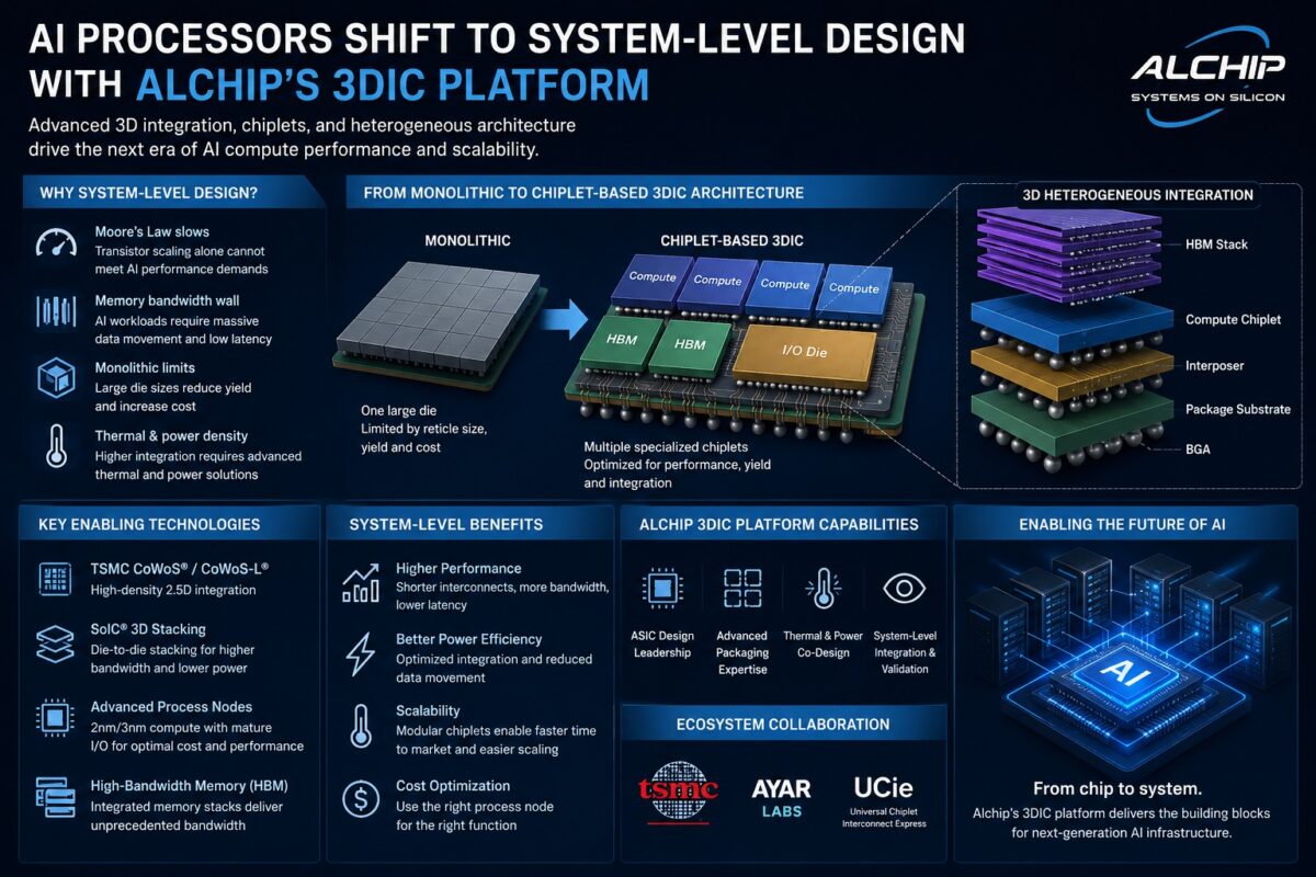
Beyond monolithic silicon.
For years, semiconductor progress marched to the drumbeat of Moore’s Law: smaller transistors, denser chips. That era, however, is effectively over for the voracious demands of artificial intelligence. AI workloads, especially generative models and hyperscale inference, now require computational power and memory bandwidth that plain old scaling can’t deliver economically or physically. What we’re witnessing is a fundamental pivot from optimizing individual chips to engineering entire systems—compute, memory, interconnect, packaging, thermals, and power delivery—as a single, cohesive architecture. This isn’t just incremental improvement; it’s a paradigm shift, and Alchip Technologies is planting its flag firmly in this new territory.
The Chiplet Revolution Gains Momentum
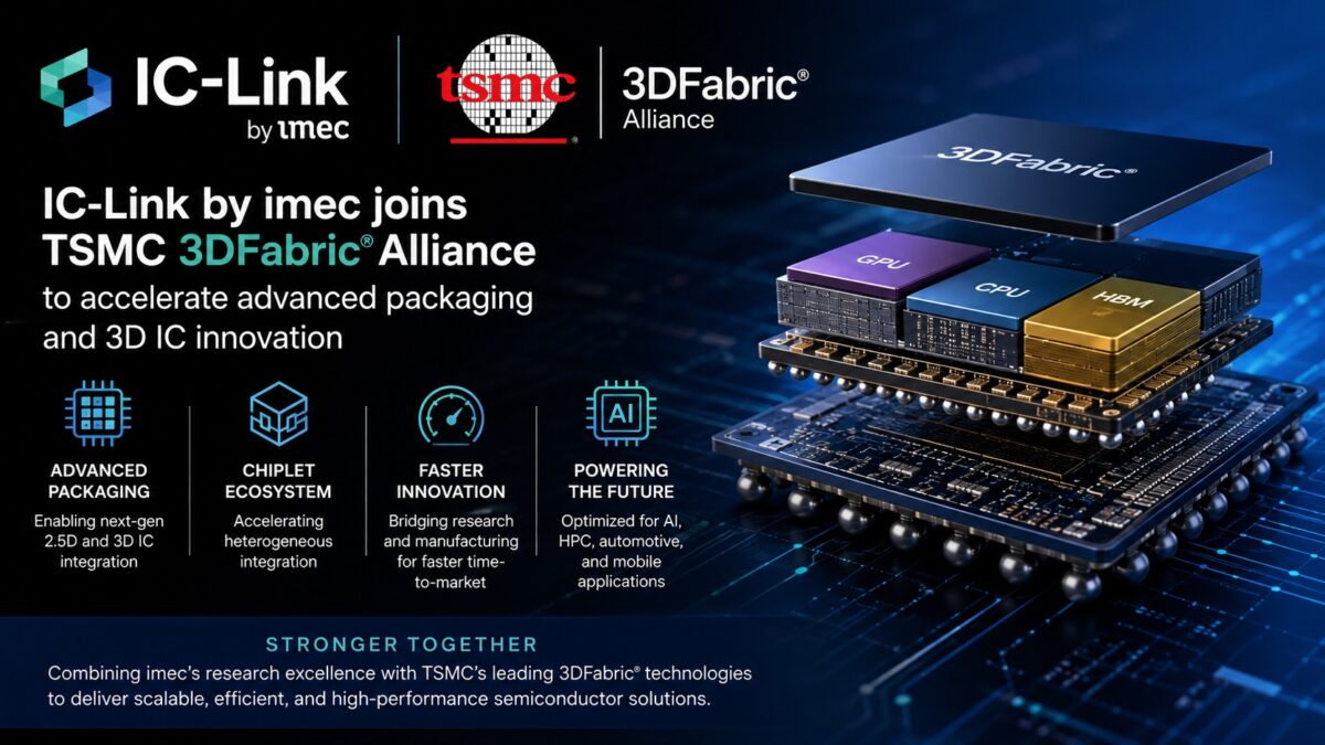
The core challenge? Monolithic dies are hitting their limits. Reticle constraints cap maximum chip size, while pushing advanced manufacturing nodes (think 3nm, 2nm, and beyond) for massive chips drastically impacts yield and cost. Building a single, giant AI processor is becoming an exercise in futility and financial risk. The industry’s elegant solution: chiplets. Instead of one gargantuan chip, designers partition functionality into smaller, specialized dies. These compute chiplets might use the bleeding edge of process technology, while less demanding I/O or memory controllers can reside on more mature, cost-effective nodes. These disparate pieces are then meticulously assembled within a single package, a feat made possible by advancements in advanced packaging.
Alchip’s 3DIC platform is the embodiment of this strategy. It’s not about designing another standalone ASIC; it’s about crafting scalable AI processor subsystems. Picture this: multiple compute chiplets, high-bandwidth memory (HBM) stacks, and dedicated I/O dies, all integrated into a unified package capable of managing multi-kilowatt power envelopes. This isn’t just assembling parts; it’s a sophisticated orchestration of silicon and packaging.
Why Is Packaging Now as Important as Transistors?
Memory bandwidth. It’s become the Achilles’ heel of AI performance. Modern AI accelerators are data hogs, demanding lightning-fast transfer rates between compute cores and HBM. Traditional packaging methods simply can’t provide the necessary interconnect density or the energy efficiency required. Here’s where advanced 2.5D and 3D packaging architectures, like TSMC’s CoWoS and SoIC, come into play. They dramatically shorten communication pathways between dies, enabling thousands of parallel connections and unlocking the data flow AI craves. Industry analysts are rightly pointing out that packaging technology is now on par, strategically, with transistor scaling itself. The intense demand for CoWoS, central to nearly every leading AI accelerator, underscores this point, creating a critical bottleneck and opportunity across the entire semiconductor supply chain. Alchip’s deep expertise in managing this complex CoWoS integration positions them squarely in one of the hottest segments of AI infrastructure.
Thermal management, once a secondary concern, is now a first-order architectural problem. As we cram more compute and memory into a single package, heat dissipation becomes a primary constraint. This necessitates a co-design approach, integrating insights from silicon, packaging, substrate engineering, and even the final cooling solutions. Alchip’s push into 2nm platforms, integrating 2nm compute dies with 3nm or 5nm I/O chiplets using advanced packaging like CoWoS-L and SoIC, exemplifies this integrated future. It’s a clear signal that the most potent AI systems won’t emerge from a single process node, but from clever, heterogeneous combinations.
The Universal Chiplet Standard is Coming
The UCIe (Universal Chiplet Interconnect Express) standard is accelerating this trend towards modularity. By standardizing die-to-die interconnects, UCIe promises a future where chiplets from different vendors can interoperate. This fosters a more flexible and potentially competitive ecosystem. Companies like Global Unichip are already demonstrating high-speed UCIe implementations, paving the way for truly composable AI hardware.
And then there’s the next frontier: optical connectivity. Alchip’s partnership with Ayar Labs to explore co-packaged optical solutions for rack-scale AI clusters hints at even greater bandwidth and efficiency gains. Integrating photonic interconnect engines directly within AI processor packages could redefine inter-chip communication for massive AI deployments.
“The industry is now shifting from chip-centric optimization toward full system-level design, where compute, memory, interconnect, packaging, thermal management, and power delivery are engineered together as a unified architecture.”
This statement, from Alchip’s own materials, perfectly encapsulates the industry’s current trajectory. It’s a stark departure from the chip-centric thinking of the past two decades. The implications are vast: for designers, it means mastering a broader range of disciplines; for hardware vendors, it opens new avenues for specialization and integration; and for end-users, it promises a future of more powerful, more efficient AI.
The AI chip design landscape is no longer a flat, monolithic plane. It’s becoming a three-dimensional, heterogeneous mix of specialized components, meticulously woven together. Alchip’s 3DIC platform isn’t just another product; it’s a concrete manifestation of this fundamental, system-level transformation. The question isn’t whether this approach will succeed, but rather how quickly the rest of the industry can adapt to this complex, yet incredibly promising, new reality. For AI, the future is integrated, and it’s happening now.