The hum of the cleanroom air, a constant, almost imperceptible thrum, usually signifies the relentless march of silicon. But lately, that sound is being overlaid by a new kind of buzz – the electrifying whisper of artificial intelligence.
The semiconductor industry, the very engine of our digital age, is facing a seismic shift. For decades, progress was a direct, almost simplistic equation: cram more transistors onto a chip. Moore’s Law, that hallowed prediction, was the gospel. But here’s the thing: the physical limits of atoms are starting to push back, like a stubborn toddler refusing to be squeezed into a smaller box. We’re talking about quantum tunneling, leakage currents, and heat that could fry an egg on a nanometer-scale wafer. It’s gotten so complex that pushing the envelope on transistor density alone has become less like an engineering feat and more like trying to perform open-heart surgery with a butter knife.
But fear not, for the future of chips isn’t dimming; it’s being re-engineered. As Dr. Jim Shiely of Siemens EDA, a key voice in the recent Beyond Moore’s Law panel, pointed out, the game is changing dramatically. It’s no longer just about the shrink wrap on the transistors.
The AI Infusion: From Tool to Foundation
Imagine a factory floor the size of a city, with thousands of complex machines performing millions of steps. Now, imagine trying to optimize that orchestra using only pre-written sheet music. That’s been semiconductor manufacturing for a while. But the sheer volume of data spewing out of these high-tech fabs – from metrology, inspection, process equipment – it’s astronomical. Terabytes upon terabytes. It’s a data tsunami. And guess what’s perfectly suited to ride that wave? Artificial intelligence.
AI isn’t just helping tweak parameters anymore; it’s becoming the central nervous system of the fab. Machine learning models are sifting through this data deluge in real time, spotting hidden correlations that would make a seasoned engineer’s head spin. They’re predicting when a multi-million dollar etching machine is about to throw a tantrum before it happens, saving precious uptime and billions in lost production. This is predictive maintenance on steroids, moving from reactive fixes to proactive, intelligent management.
Design Meets Destiny: The Rise of Co-Optimization
Historically, chip designers and the folks building the fabs operated in parallel universes, occasionally throwing blueprints over the fence. That era is officially over. We’re now in the age of design-technology co-optimization (DTCO). Think of it like this: a chef doesn’t just invent a recipe; they consider the available ingredients, the oven’s quirks, and the plating style all at once. Chip design and manufacturing are now intertwined from the ground up.
AI is proving to be an indispensable sous-chef in this culinary-tech kitchen. AI-assisted EDA (Electronic Design Automation) tools are accelerating everything from placing millions of transistors to ensuring the chip won’t melt under load. And generative AI? It’s starting to draft designs, predict defects before they even manifest physically, and slash engineering iteration cycles – which, in this industry, is like finding a cheat code for time.
“Rather than relying solely on lithographic shrink, semiconductor progress is now driven by system-level efficiency, packaging technologies, and intelligent manufacturing ecosystems.”
This quote, from the panel discussion, perfectly encapsulates the paradigm shift. It’s about building smarter systems, not just smaller components.
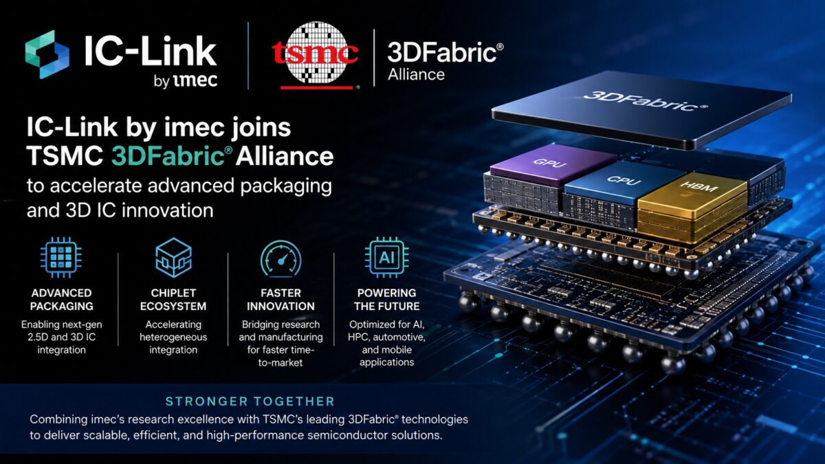
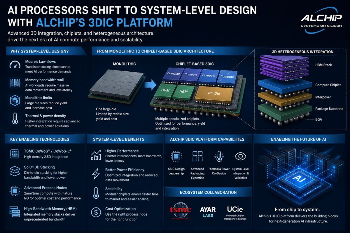
Advanced Packaging: Building Up, Not Just Out
So, if shrinking transistors is hitting a wall, how do we keep boosting performance? Enter advanced packaging – the unsung hero of the post-Moore’s Law era. Forget the flat, single-chip approach. We’re talking about stacking. Chiplets, 2.5D integration, 3D stacking – these are the new frontiers.
Imagine taking specialized chips – a CPU here, a GPU there, some lightning-fast memory, a dedicated AI accelerator – and snapping them together like high-tech LEGOs. This isn’t just about fitting more on a board; it’s about creating incredibly efficient, powerful systems where specialized components work in perfect harmony. For AI workloads, where memory bandwidth and how quickly data can zip between components are often the real bottlenecks, this architectural leap is nothing short of critical.
The Data Backbone: Fueling the Future
All this intelligence, all this complexity, all this advanced packaging – it all runs on data. And not just any data. We need infrastructure that can keep pace, offering low latency and massive scalability. Think of it as the circulatory system of the modern fab. High-performance parallel file systems, cloud-integrated storage architectures… these are no longer nice-to-haves; they’re absolute necessities.
And then there are digital twins. These aren’t just simulations; they’re virtual replicas of the entire manufacturing process, allowing engineers to experiment, optimize, and innovate at light speed without risking a single physical wafer. It’s like having a sandbox for innovation on an industrial scale.
Resilience and Security: The New Imperatives
The semiconductor supply chain is notoriously global and complex. A hiccup in one corner of the world can ripple outwards with devastating effect. AI is increasingly being deployed to bring visibility to this complex web, predicting disruptions, optimizing inventory, and making production more resilient. But as these systems become more interconnected and cloud-enabled, the stakes for cybersecurity skyrocket. Protecting IP and manufacturing data isn’t just good practice; it’s existential.
The future of semiconductor manufacturing isn’t a simple continuation of the past. It’s a radical reimagining, powered by AI, fueled by data, and structured by ingenious new packaging techniques. The old playbook is gathering dust. The new one is being written, line by complex, intelligent line, right now.
Why Does This Matter for Developers?
This shift means that developers are going to have access to increasingly powerful and specialized hardware. The integration of chiplets and heterogeneous computing means systems can be tailored for specific tasks—think AI development, scientific simulation, or graphics rendering—with unprecedented efficiency. Understanding how these specialized components work together will become more important, opening up new avenues for optimizing software performance. Furthermore, the increased use of AI in design and manufacturing could eventually lead to faster access to cutting-edge silicon, as the design and production cycles are streamlined.
The AI Platform Shift Is Here
It’s easy to get lost in the technical jargon of lithography and wafer yields. But the real story, the seismic undercurrent, is that we’re witnessing another fundamental platform shift, akin to the advent of the internet or the mobile revolution. AI isn’t just a feature being bolted onto existing systems; it’s becoming the foundational operating system for entire industries, and semiconductor manufacturing is one of the most critical proving grounds. The innovations discussed aren’t incremental; they’re creating entirely new paradigms for how we design, build, and utilize the very chips that power our world. This isn’t just about faster phones or more powerful GPUs; it’s about redefining what’s possible at the silicon level, and the implications will cascade through every sector of technology and beyond.
🧬 Related Insights
- Read more: PCB Signoff Finally Gets Smart, Or Just Faster?
- Read more: cuTile BASIC: NVIDIA Makes GPUs Speak 1970s Code – And It Runs Lightning Fast
Frequently Asked Questions
What is the biggest challenge facing semiconductor manufacturing today? The biggest challenge is the physical limitation of traditional transistor scaling, making it increasingly difficult and expensive to improve performance through density alone. Innovations are now focused on system-level efficiency, advanced packaging, and AI-driven optimization.
How is AI being used in semiconductor manufacturing? AI is being used to analyze vast amounts of manufacturing data to optimize processes, predict equipment failures (predictive maintenance), accelerate chip design through EDA tools, and improve overall yield and efficiency in the fab.
What is advanced packaging in chipmaking? Advanced packaging refers to techniques that go beyond traditional chip design, such as chiplets, 2.5D integration, and 3D stacking, to combine multiple specialized chips into a single, high-performance system. This allows for performance gains without solely relying on shrinking transistor sizes.