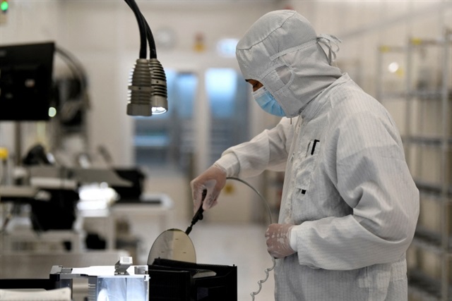
Sweat beads on an engineer’s forehead in a sterile Menlo Park lab. The laser probe hits the chiplet stack; temps rocket past 150°C in a layer no thicker than a virus.
Thermal metrology. There, I said it—right up front, because this whitepaper promo from Laser Thermal screams it like a bad infomercial. But hey, they’re onto something. Next-generation semiconductors aren’t just shrinking; they’re stacking into feverish 3D mazes where heat doesn’t flow, it festers.
Classical assumptions? Dead on arrival.
Why Do Nanoscale Films Laugh at Bulk Thermal Math?
Engineers used to model heat like water through a pipe—simple, bulk properties, done. But at nanometer thicknesses, that’s fantasy. Thin films, funky materials, power densities spiking like a bad crypto pump. Heat conductivity tanks, models lie, and your gate-all-around transistor turns into a toaster.
Take this gem from the whitepaper:
As devices scale into three-dimensional architectures with thinner layers, higher power densities, and increasingly complex material stacks, heat transport becomes confined, interface-dominated, and highly sensitive to small variations in structure and processing.
Spot on. But Laser Thermal’s sponsoring this—smells like a pitch for their laser toys. Still, ignore the sales, absorb the pain.
Here’s my twist nobody else mentions: this echoes the 90s power wall that killed off-the-wall clock speeds. Back then, Dennard scaling cracked; heat per transistor exploded. Today? Vertical stacks bury the problem deeper. Prediction: without metrology upgrades, 3D chiplets flop like Itanium—hyped, hot, history.
Short para for punch: Brutal.
Buried Heat Traps in 3D Stacks—Nightmare Fuel?
3D integration. Gate-all-around. Backside power delivery. Sounds futuristic, right? Wrong—it’s a thermal chokehold. Vertical heat flow? More like vertical prison. Bonded interfaces, TIM layers, dielectrics—they’re the new bosses, slapping thermal boundary resistance on everything.
Power densities climb, layers thin to atoms, and suddenly a 2nm variation in processing spikes resistance 50%. Models without real measurements? Garbage in, fab disaster out. Late-stage redesigns? Millions flushed.
And the hype—oh, the corporate spin. “Thermal-first design workflow,” they coo. Translation: measure everything, or watch reliability crater. I’ve seen packages delaminate in qual tests; it’s ugly, like popcorn in a microwave.
But wait—spatial variability. Heat doesn’t spread even; hotspots lurk in “buried thermal bottlenecks.” Classical metrology—slap a thermocouple, call it good? Laughable. You need scale-appropriate tools, probing films and interfaces without wrecking the die.
Is Thermal Metrology Ready for Chiplet Chaos?
Heterogeneous integration. Chiplets glued like a Frankenstein puzzle. Each interface a resistance roulette. Whitepaper nails it: “thermal boundary resistance at bonded interfaces… has become a first-order driver of performance limits.”
Yet industry’s asleep. Fabs churn 3D stacks assuming old data. Result? Systems throttle under load, or worse, fail early. Remember Intel’s 20A backside power reveal? Bold move, but thermal metrology lags. Without it, it’s PR gloss over physics.
Unique gripe: this whitepaper’s a wake-up, but sponsored. Laser Thermal wants your budget—fair, their transient thermoreflectance sounds slick. But don’t buy the sizzle; demand proof. History says heat always wins; bet against it, lose big.
Workflow shift needed. Measure thin films. Validate models. Cut uncertainty. Or embrace the redesign merry-go-round.
One sentence: Overdue.
Dense dive: Emerging materials—wide-bandgap like GaN, 2D stuff like MoS2—throw curves. Stacks mix silicon, glass, organics; thermal paths zigzag. Metrology must evolve: picosecond lasers, non-contact, nanoscale resolution. Otherwise, AI accelerators? Cooked. HPC? Throttled. Phones? Battery vampires.
The Real Cost of Ignoring Heat
Long-term reliability. That’s the kicker. Hotspots migrate defects, accelerate electromigration. Your “reliable” package? Infant mortality waiting.
Thermal-first ain’t optional—it’s survival. Whitepaper pushes measured properties over guesses. Smart. But execution? Fabs hoard data; vendors spin. Skeptic’s call: open-source thermal benchmarks, or we’re all flying blind.
Bold prediction: by 2027, thermal metrology startups boom, or TSMC/Samsung dictate standards amid failures.
🧬 Related Insights
- Read more: C-BATT’s Obsidia Anode Swells Only 2-5%—Half Graphite’s Rate—Nabs Top Award at Battery Seminar
- Read more: Linux Kernel 7.1 Kicks Intel 486 to the Curb After 35 Years
Frequently Asked Questions
What is thermal metrology in semiconductors?
It’s measuring heat flow at nano-scales—conductivity, resistance in films and interfaces. Old tools fail; new ones probe without touch.
Why does thermal metrology matter for 3D chips?
3D stacks trap heat in buried layers; ignore it, and performance tanks, reliability dies. Essential for modeling and design.
Can current thermal tools handle next-gen semis?
Nope—bulk assumptions crumble. Need advanced laser-based metrology for thin films and bonds.