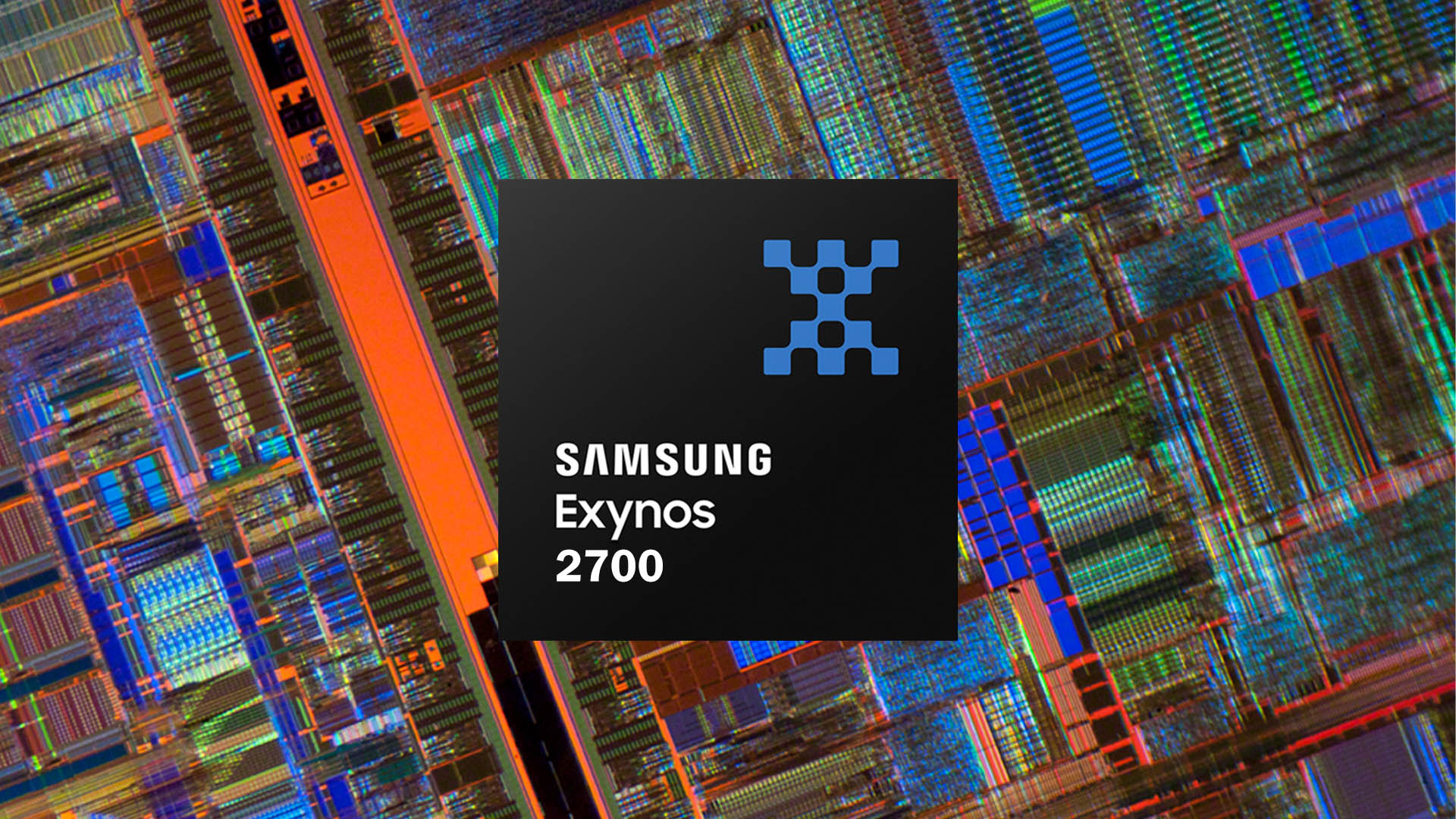
Samsung’s SoC abandonment? No.
For a while there, the tech ether was buzzing with a rather unsettling narrative: Samsung, facing pressure from a supposed DRAM shortage and the relentless pursuit of affordability, was apparently ready to ditch its most advanced packaging techniques for its next-generation Exynos chipset, the Exynos 2700. This meant potentially sidelining Fan-Out Wafer-Level Packaging (FOWLP), a technology that, while pricey, offers significant gains in size, thermal performance, and overall chip efficiency. The implication? A less potent, more cost-conscious chip for the upcoming Galaxy S27 series.
But hold on. A new wave of chatter, originating from the rather shadowy corners of tech rumor mills (specifically, a user named @SPYGO19726, whose credibility remains, shall we say, an open question), is pushing back. The story now is that Samsung isn’t just not abandoning FOWLP for the Exynos 2700; it’s doubling down. The company, according to these claims, is committed to giving its 2nm SoC the absolute best of its in-house technologies, a move designed to go toe-to-toe with the likes of Qualcomm’s Snapdragon and MediaTek’s Dimensity powerhouses. This isn’t just about making a chip; it’s about making a statement.
Why Does FOWLP Matter So Much?
Look, it’s easy to gloss over terms like “Fan-Out Wafer-Level Packaging.” It sounds arcane, a detail for engineers tucked away in sterile labs. But the reality is, these advanced packaging techniques are becoming increasingly critical differentiators in the mobile SoC arms race. FOWLP, in particular, allows for more complex interconnections between different chip components and even separate dies on a single package. Samsung claims that adopting FOWLP can lead to chips that are up to 40 percent smaller and 30 percent thinner, all while boasting a 16 percent improvement in thermal resistance. Think about that: a smaller, cooler chip that can sustain higher clock speeds for longer periods. For demanding tasks like mobile gaming, AI processing, or even just snappy multitasking, that’s the difference between a frustrating stutter and a buttery-smooth experience.
FOWLP not only helps make chipsets 40 percent smaller, but they also boast 30 percent lower thickness while flaunting 16 percent improved thermal resistance.
This isn’t just about bragging rights in spec sheets. It’s about unlocking new levels of performance and efficiency that direct silicon scaling alone can’t always deliver. And when you combine this advanced packaging with Samsung’s own cutting-edge 2nm Gate-All-Around (GAA) process, the potential for the Exynos 2700 to be a genuine contender against its rivals becomes much more tangible.
The company’s stated goal with this approach, especially with the rumored integration of a new side-by-side (SBS) architecture to manage heat transfer between CPU and DRAM, is clear: to ensure the Exynos 2700 can handle taxing workloads without thermal throttling. This is the kind of architectural thinking that separates good chips from great ones, and it’s what consumers ultimately experience as tangible performance benefits.
Corporate Drama or Genuine Intel?
Now, here’s where things get truly interesting, and perhaps a bit speculative. The source of the new information, @SPYGO19726, posits something rather audacious: the original reports about Samsung ditching FOWLP were not merely misguided but deliberately fabricated. The motive? To tarnish Samsung’s reputation. Why? According to this theory, it’s linked to internal labor disputes. The claim is that disgruntled employees, wanting a larger slice of Samsung’s considerable profits, are orchestrating a campaign of disinformation. It’s a dramatic narrative, bordering on industrial espionage, that could potentially explain why such a report would gain traction. It also begs the question of how such a report, even if false, managed to get picked up by reputable outlets like Sisajournal in the first place.
This whole saga highlights a recurring theme in the high-stakes semiconductor industry. Companies are constantly battling not just technological challenges but also perceptions. PR spins, carefully crafted leaks, and even outright disinformation campaigns can shape market sentiment and influence investor and consumer opinion. The fact that Samsung, or at least sources close to them, feel compelled to publicly refute these claims suggests the potential damage was seen as significant.
The Cost of Innovation
Of course, the elephant in the room remains cost. FOWLP is undeniably expensive. Integrating it requires specialized equipment and processes, and it’s a significant contributor to the overall bill of materials for a high-end chip. This is precisely what fueled the initial rumors – a cost-cutting imperative. While @SPYGO19726 seems convinced that Samsung will stick with FOWLP, the potential for a last-minute pivot remains. Chip manufacturing is a complex, multi-stage process, and decisions can be revisited as production ramps up and final costs become clearer. It’s entirely possible that while the intent is to keep FOWLP, economic realities could force a change by the time the Exynos 2700 hits mass production.
But for now, the narrative has shifted. The Exynos 2700 is slated to receive the full premium treatment, promising a more competitive Samsung silicon offering. It’s a crucial development for Samsung’s mobile division, which has struggled to consistently match Qualcomm’s flagship performance in recent years. If the Exynos 2700 lives up to its potential, it could significantly bolster the appeal of future Galaxy devices and perhaps even signal a broader resurgence for Samsung’s own chip designs.