So, the semiconductor industry’s crystal ball usually shows us next year’s phone chip is a smidge faster, a hair smaller. We expected more of that. Imec, a Belgian nanotech research outfit that actually knows what it’s talking about—unlike your average PowerPoint-wielding CEO—just pulled back the curtain on its 15-year roadmap. And frankly, it makes our current silicon dreams look quaint.
Forget what you think you know about transistors. The next big thing, slated for a commercial debut around 2033, is something called a Complementary FET, or CFET. Sounds like jargon? It is. But here’s the gist: it’s a way to cram two transistors into the space of one. Because apparently, side-by-side wasn’t enough. We’re talking about stacking them. Think of it as vertical farming for your logic circuits.
And if that doesn’t twist your silicon-loving brain into knots, hang on. Imec is also predicting another seismic shift around 2041. This one’s all about power reduction, which, let’s be honest, is the real battleground now. They’re talking about ditching the main silicon part of the transistor—the channel—for two-dimensional semiconductors. Materials so thin they’re practically ghosts, like molybdenum disulfide. A single atomic layer thick. Yes, you read that right. We’re going two-dimensional.
Is This Just Wishful Thinking or a Real Roadmap?
Fifteen years is an eternity in tech. Most roadmaps crumble after five. But Imec’s projections aren’t just pulled from a hat. Paul Heremans, their CTO, explained their role. They’re the de-riskers. They poke and prod these wild ideas, figuring out if they’re even possible, and at what cost. This isn’t about product launch cycles; it’s about foundational research that chip giants like Intel, Samsung, and TSMC depend on. They need years, sometimes decades, to translate these lab experiments into something you can buy.
So, while CFETs are the focus for 2033, the real heavy lifting is happening now to make them work. The current plan? Build both transistor types—the PMOS and NMOS duo that makes modern computing tick—simultaneously, not sequentially. Imagine layering silicon and silicon germanium, then etching away the germanium to leave behind suspended silicon ribbons. These ribbons become your stacked transistors. It’s complex. It’s messy. And it’s already in prototype.
“It is very clear that there are many versions still open.”
Heremans isn’t kidding. The exact flavor of CFET is far from settled. Imec is wrestling with how to keep the top and bottom transistors electrically separate, a surprisingly difficult problem. One approach involves bonding two separate wafers, each optimized for its transistor type, then peeling off the excess. This sounds like a recipe for disaster, yet it might also solve speed mismatches between PMOS and NMOS. Intel, bless their persistent hearts, is apparently trying this very scheme.
Why Does the 2041 Prediction Matter Now?
Predicting something for 2041 is usually a fool’s errand. But Imec’s timeline for 2D semiconductors isn’t just a random date. It follows a familiar pattern: FinFETs debuted about 15 years ago, and nanosheet transistors are just now hitting the market. This new projection suggests that the move to truly exotic materials, far beyond silicon as we know it, is not just a possibility but a planned evolution. It’s a clear signal that the industry is already thinking about what comes after the post-silicon era, even if that era isn’t quite here yet.
The implications are staggering. We’re talking about materials that are thinner than a human hair’s width. Semiconductors that could enable entirely new forms of computing, perhaps even tackling the immense power demands of AI without melting our power grids. This isn’t just about cramming more transistors; it’s about fundamentally changing the building blocks of computation.
Of course, there’s always the skeptical eyebrow. Imec’s roadmap is a guide, not a guarantee. The journey from lab concept to mass production is littered with discarded ideas and economic realities. Companies will chase the most profitable path, not necessarily the most scientifically elegant one. Still, when a group like Imec, with its track record, lays out such a bold vision, it’s worth paying attention. They’re not just reporting on the present; they’re sketching out the blueprint for the future.
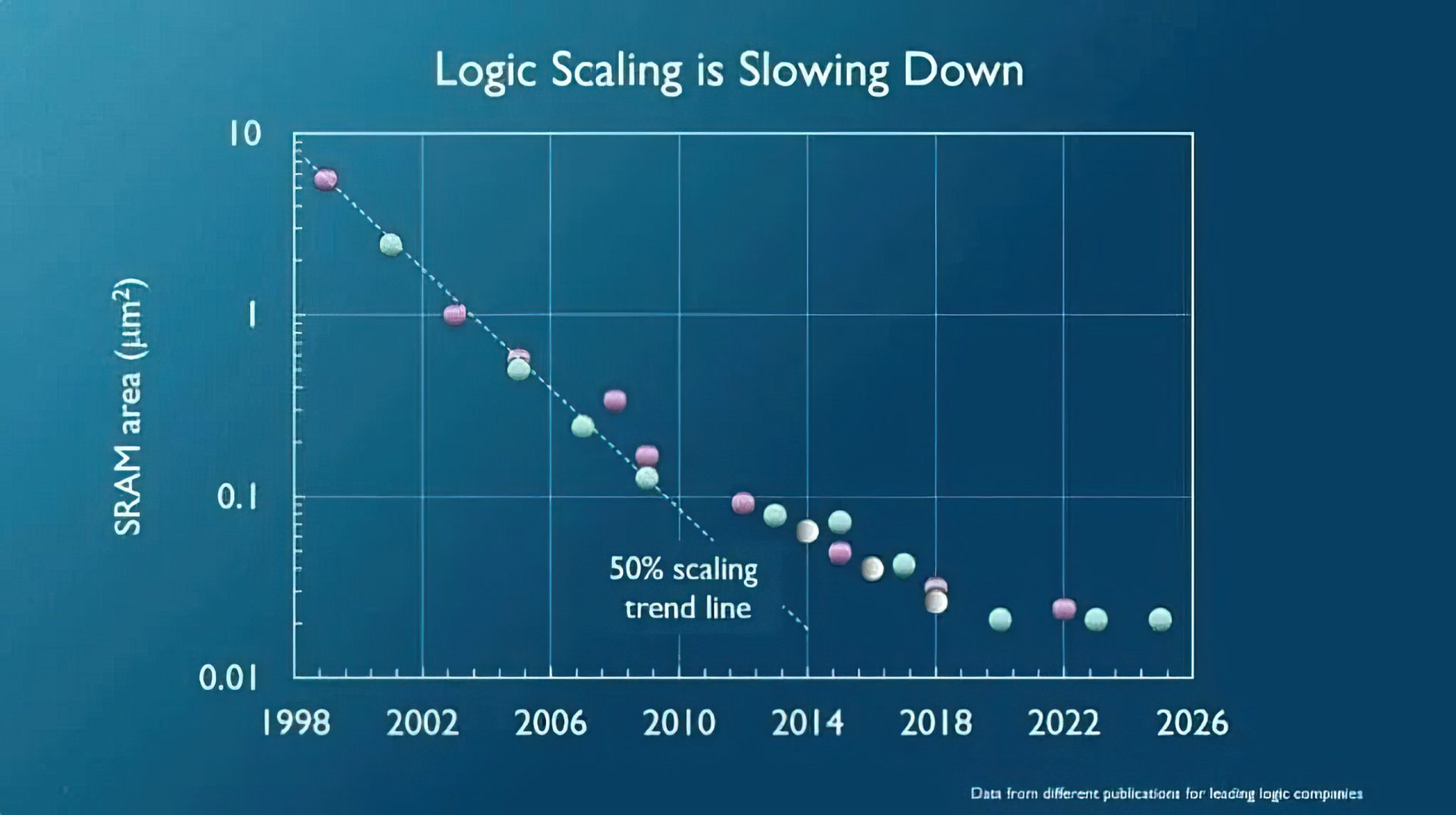
What’s the big takeaway? Moore’s Law, in its most literal sense, might be groaning under the strain. But the spirit of Moore’s Law—the relentless drive for more performance, less power, and smaller footprints—is very much alive. It’s just getting incredibly inventive, and perhaps a bit terrifyingly, in its methods. We’re not just scaling down; we’re stacking up and layering down to atomic thinness. Hold onto your hats. The next 15 years are going to be wild.