Here’s the thing: we’ve all heard the whispers, the pronouncements that Moore’s Law is dead, or at least gasping for air. But progress, as it always does, finds a way. The latest roadmap from IMEC, the undisputed titan of nanoelectronics research, doesn’t just confirm the slowdown; it meticulously charts a new, elongated course through the sub-2nm and eventually the sub-1nm territories.
It’s a future arriving incrementally, with sub-1nm process nodes now projected for around 2034. This isn’t a sudden leap, but a calculated crawl. The journey from our current sub-2nm ambitions to the theoretical bleeding edge of 0.2nm and beyond, well, that’s a marathon extending to 2046. This isn’t just about smaller transistors; it’s about entirely new ways of building them.
The Slow Burn Towards Angstroms
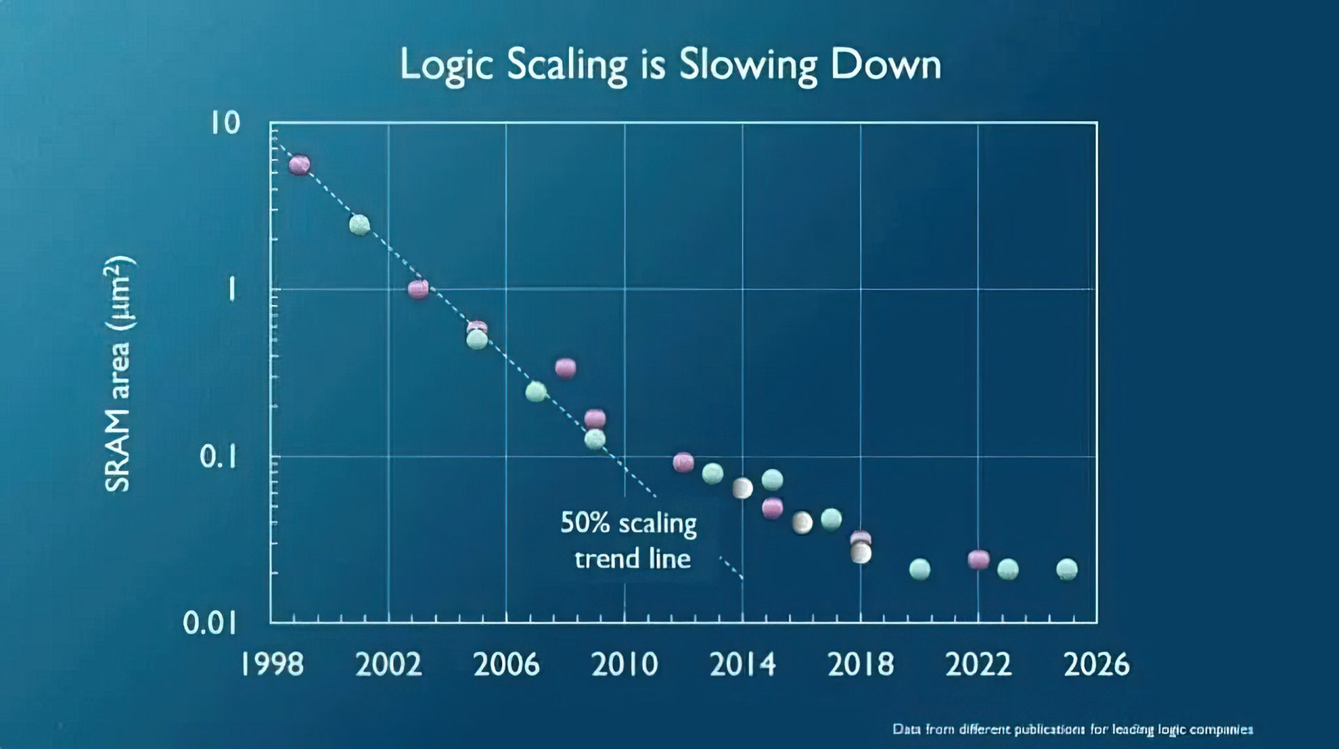
The semiconductor industry’s relentless pursuit of density has hit a wall, or perhaps more accurately, a very expensive, atomically precise barrier. While newer nodes continue to offer performance gains, the cost of entry — and the complexity of the machinery required — has skyrocketed. We’re seeing an increasing reliance on advanced packaging solutions, the ‘chiplet’ approach, as a pragmatic way to stitch together more powerful systems without necessarily jumping to the absolute cutting edge of process technology. This has, in effect, eased the immediate pressure to shrink.
But IMEC, the Belgian research powerhouse, sees beyond the immediate. Their latest ‘Logic Device Roadmap’ paints a picture of where the fundamental silicon innovations are headed, stretching from the 2020s all the way to the mid-2040s. These aren’t production schedules; they’re targets for technological development completion, a beacon for the industry’s R&D efforts.
Nanosheets and the Sub-2nm Prelude
The immediate future is dominated by ‘Nanosheet’ FETs, also known as Gate-All-Around (GAA) transistors. This is the technology underpinning TSMC’s N2 node, which is already in mass production as I write this. Intel is also pushing hard with its own iterations, like the A16 and 14A processes. These Nanosheet designs represent a significant architectural shift, offering better gate control and reducing leakage compared to FinFETs. However, they are still within the realm of what we’ve come to expect as ‘sub-2nm’. The roadmap suggests A10, the last Nanosheet-based node, will pave the way for the sub-1nm era around 2031.
Stacking Up: The Rise of CFETs for Sub-1nm
This is where things get truly interesting. To breach the sub-1nm barrier, the industry is looking at Complementary FETs, or CFETs. Imagine taking those Nanosheet transistors and stacking them vertically. The concept is elegant: shrinking the footprint by building up rather than just out. This approach promises a significant boost in transistor density, potentially up to 80% increase for CMOS logic circuits.
The first process node featuring CFETs is expected by 2034 and is going to offer the first sub-1 nm process tech.
The projected timeline shows a staggered rollout: A7 (0.7nm) by 2034, followed by A5 (0.5nm) by 2036, and A3 (0.3nm) by 2040. This isn’t just an incremental refinement; it’s a fundamental reimagining of transistor layout at the atomic scale.
The Angstrom Frontier: 2D FETs and New Materials
But IMEC’s gaze extends even further, into the truly exotic ‘2 Angstrom’ era. This is where we’ll likely see the advent of 2D FET technology. Think beyond stacked nanosheets; we’re talking about ultrathin, two-dimensional materials forming the very core of the transistors. This will necessitate entirely new materials science breakthroughs and fabrication techniques. The roadmap calls for the first application of 2D FETs in an A2 (0.2nm) node by 2043, with technologies pushing below this threshold (<0.2nm) arriving by 2046.
This shift will require equally radical changes in the interconnects. The current Dual-Damascene and Single-Damascene processes using copper will give way to Semi-damascene / Subtractive Metallization approaches for sub-1nm nodes. We’re talking about using materials like Ruthenium (Ru) to replace copper, enabling barrierless vias for reduced resistance and better conductivity. For the even more advanced 0.5nm and sub-nodes, IMEC hints at materials like Epitaxial PtCoO₂ on Sapphire.
What strikes me here isn’t just the timeline, but the architectural pivot. The move from 2D planar structures to FinFETs, then to Nanosheets, and now to stacked CFETs and potentially 2D materials, represents a profound architectural evolution. We’re not just scaling down; we’re redesigning the very fabric of computation at the most fundamental level. The implications for power, performance, and even the types of computation we can achieve are vast. This isn’t just an iterative update; it’s a foundational redesign of the silicon continent.
Why Does This Matter for System Designers?
For those building the next generation of systems, whether for AI, HPC, or edge devices, this roadmap is a vital, albeit long-term, guide. The increasing complexity and cost of leading-edge nodes mean that advanced packaging and system-level co-design will remain paramount. However, the eventual availability of these ultra-dense nodes — even decades out — opens up possibilities for entirely new device paradigms. Designers will need to anticipate these architectural shifts, understanding how CFETs and 2D FETs will influence interconnect, power delivery, and thermal management. The gap between research and production is substantial, but the direction of travel is clear, and it’s a fascinatingly complex one.
🧬 Related Insights
- Read more: AMD CPU + 32GB DDR5 RAM Bundle Drops to $830
- Read more: PCB Signoff Finally Gets Smart, Or Just Faster?
Frequently Asked Questions
What is IMEC? IMEC is a world-leading independent research and innovation center for nanoelectronics and digital technologies, based primarily in Belgium.
When will sub-1nm process technology be available? IMEC’s roadmap suggests the first sub-1nm process technology, featuring CFETs, is expected around 2034.
What is 2D FET technology? 2D FET technology involves using ultrathin, two-dimensional materials to form transistors, representing a significant architectural shift beyond current nanosheet and CFET designs, expected around 2043.