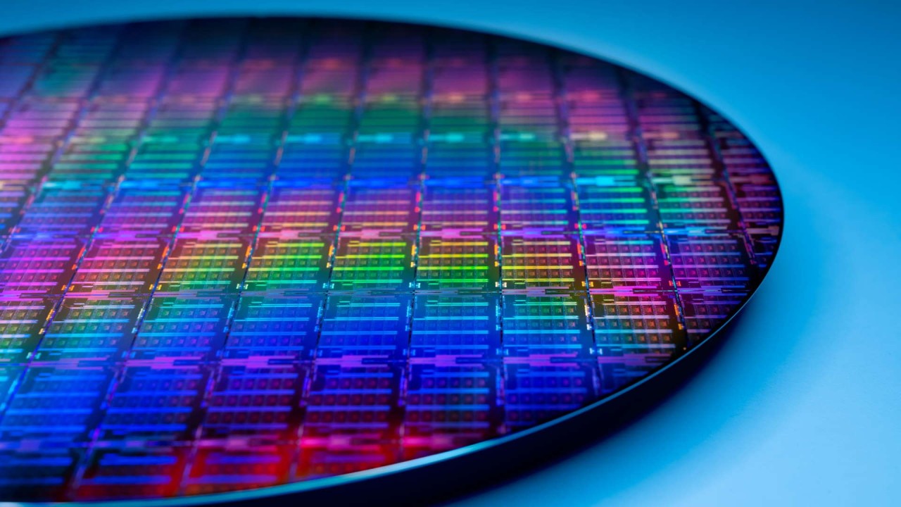
When will chips actually get small again? You know, smaller than a nanometer? It’s a question that seems to have been lost in the shuffle of more cores, more AI accelerators, and frankly, more expensive silicon. But the folks at IMEC, the European semiconductor research giant, are still crunching the numbers, and they’ve laid out a timeline that suggests we’re staring down the barrel of truly Angstrom-scale fabrication by the mid-2030s, with even wilder possibilities looming in the 2040s. Don’t hold your breath for your next iPhone, though. This is the research frontier, not the factory floor, and the journey is proving… arduous.
The Angstrom Era Is Coming. Eventually.
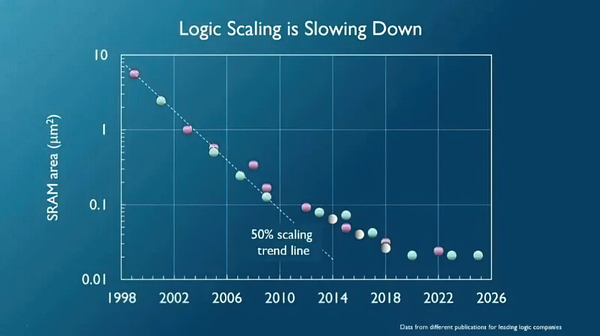
Let’s be clear: Moore’s Law, in its original, glorious, doubling-every-two-years form, is about as relevant as a dial-up modem. We’ve seen scaling slow to a frustratingly linear pace. It’s been years since we’ve seen a genuine leap in density that didn’t require a second mortgage for the machinery. This slowdown isn’t for lack of trying. It’s the physics, stupid. And the economics. Every single shrink costs more than the last, and the benefits—well, they’re getting harder to justify on a per-transistor basis.
But demand doesn’t care about physics or economics. The insatiable hunger for more performance, especially in AI and high-performance computing, means the industry has to push forward. So what do we do? We get creative. Advanced packaging, like chiplets and TSMC’s ambitious System-on-Wafer (SoW), are the current stopgaps. They let us build bigger, more powerful systems by stitching together smaller, specialized chips. It’s smart. It’s cost-effective. It buys the foundries time to figure out how to etch things smaller than a virus.
“The year respective to the process node does not indicate a production timeframe, but links to the development completion of the technology.”
This is the crucial caveat from IMEC’s roadmap. These dates aren’t when you’ll be buying your next quantum-leap smartphone. They’re when the fundamental technology is expected to be debugged, demonstrated, and ready for the agonizingly slow process of industrialization. We’re talking development completion.
Nanosheets: The Last Gasp of 2D Scaling?
Before we get truly wild, IMEC’s roadmap points to the continued evolution of what they call “Nanosheet” transistors, the GAA (Gate-All-Around) architecture that’s already starting to appear with TSMC’s N2 node this year. These are the workhorses that will likely carry us through the late 2020s and into the early 2030s. Think of them as a refinement, a stretching of existing design principles to squeeze out a bit more performance and density. TSMC and Intel are both betting big on variations of this. The roadmap suggests the last of these Nanosheet-era nodes, maybe an A10 equivalent, will be around 2031. After that? We need something fundamentally different.
The Sub-1nm Horizon: Vertical Stacking and CFETs
Here’s where things get interesting. To break the 1nm barrier, IMEC predicts the rise of Complementary FETs (CFETs). The concept? Stack those nanosheet transistors vertically. Imagine a tiny skyscraper instead of a sprawling single-story building. This vertical integration promises a significant boost in transistor density—up to 80% according to IMEC.
The first node using CFETs is penciled in for 2034, targeting a sub-1nm process. Following that, we see targets for 0.5nm by 2036 (A5) and 0.3nm by 2040 (A3). This isn’t just about fitting more transistors; it’s about fundamentally rethinking the layout at the atomic level. The BEOL (Back-End-of-Line) scaling, the stuff that connects all these transistors, also needs an overhaul. Expect to see Ruthenium replacing copper for better conductivity and novel materials like Epitaxial PtCoO₂ on Sapphire for the really deep cuts. It’s a whole new ballgame for interconnects.
2D FETs: The Real Frontier by 2046?
But wait, there’s more. For the true far-future enthusiasts, IMEC is looking at 2D FET technology for nodes around 0.2nm and below, slated for 2043 and 2046. This involves entirely new materials—actual two-dimensional materials—forming either 2D CFETs or 2D Nanosheet structures. This is where the science fiction truly begins to intersect with engineering. We’re talking about materials that are literally one or two atoms thick. The challenges here are monumental, not just in fabrication but in understanding the fundamental material properties and how to reliably integrate them. The roadmap acknowledges this is highly theoretical, and a lot can change. Frankly, I’d be surprised if it all lands precisely on those dates.
The semiconductor industry has a habit of pulling rabbits out of hats. But the pace of innovation, while still impressive in its own way, is a marathon now, not a sprint. These sub-1nm nodes are a proof to human ingenuity, yes, but also a stark reminder that physics imposes its will. The future of computing is smaller, denser, and a whole lot more complicated than we ever imagined.
🧬 Related Insights
- Read more: Photonic Computing: How Optical Chips Could Transform Data Processing
- Read more: Intel and CrowdStrike Unlock Secure AI on Every PC
Frequently Asked Questions
What is IMEC? IMEC is a world-leading independent research and innovation hub in nanoelectronics and digital technologies, based in Belgium. They work with industry partners to develop advanced semiconductor technologies.
Will these sub-1nm chips be available soon? No. The IMEC roadmap highlights development completion timelines, not mass production dates. Sub-1nm technology is not expected to be widely available until well after 2034, with the most advanced concepts pushing into the late 2040s.
How is this different from current chip technology? Current leading-edge chips use 3D structures like FinFETs and Nanosheets. Sub-1nm technologies involve fundamentally new architectures like vertically stacked Complementary FETs (CFETs) and potentially exotic 2D materials, aiming for vastly increased transistor density at atomic scales.