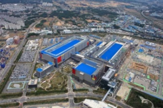
Here’s a number to chew on: $5 billion. That’s how much Applied Materials is reportedly throwing at its new EPIC Center. And for what? To solve the increasingly messy problem of building the chips that power our insatiable AI appetite. It’s the biggest commitment to semiconductor equipment R&D in US history, according to the company. You don’t drop that kind of cash without seeing a serious problem, and folks, the problem is real.
We’re talking about the energy-efficient AI era, a concept that sounds nice but boils down to a brutal engineering reality: moving data around is a massive energy hog. Compute itself is only part of the story; the bits zipping across circuits can drain power just as fast, if not faster. So, while everyone’s busy bragging about teraflops and petaflops, the real fight is happening at the system level, where logic, memory, and advanced packaging all have to play nice.
Think of it: your fancy new logic chips need memory that can keep up, but they’re often separated by a chasm. Then you’ve got advanced packaging, the fancy 3D stacking and chiplet wizardry, trying to cram everything together. But none of it works if the fundamental pieces – the transistors, the wires, the very materials – aren’t perfectly integrated. It’s a Gordian Knot of interdependence, and the old way of doing things, that slow, siloed R&D relay race, just isn’t cutting it anymore.
The Relay Race is Too Slow
For decades, chipmaking innovation followed a predictable path: develop a component, hand it off, let someone else integrate it, get some feedback, and start over. It worked when steps were independent. Now? Not so much. At the angstrom scale – we’re talking about individual atoms here – everything is linked. Material choices dictate how you stack things, which dictates design rules, which dictates power, which dictates thermal budgets, which ultimately constrains how small you can make things. You can’t just plug and play anymore.
And the AI timeline? It’s been compressed into warp speed. System architects don’t have 10-15 years to wait for the next big semiconductor inflection. They need it yesterday. This is where Applied Materials’ EPIC Center comes in – a supposed platform for “high-velocity co-innovation.”
The EPIC model compresses the traditional workflow. Customer engineers Can collaborate with Applied Materials experts on-site in a facility Designed to shorten the cycle time from materials innovation to pilot Production.
Essentially, they’re trying to build a giant, shared playground for the big players – companies and academics alike – to hash out these boundary-spanning problems together. The idea is to collapse those feedback loops, shorten the timeline from lab bench to fab floor, and get everyone on the same page, simultaneously. It’s a massive bet that throwing money and a bunch of smart people into the same room, with the right tools, will magically speed up innovation.
Who’s Actually Making Money Here?
Let’s be clear: Applied Materials isn’t doing this out of the goodness of its corporate heart. Their business is selling the equipment that makes these incredibly complex chips. If they can engineer a faster, more efficient way to innovate, they sell more machines. If their customers can build better, faster AI chips because of EPIC, they’ll need even more cutting-edge equipment. It’s a classic ecosystem play, but with a five-billion-dollar price tag, the pressure is on.
The real question is whether this centralized, co-innovation model, as impressive as the investment sounds, can actually overcome the deep-seated historical silos and competitive pressures that have defined the semiconductor industry. Can they truly collapse learning loops when everyone is still ultimately trying to get ahead of their rivals? It’s a bold experiment, certainly. Whether it’s a successful one remains to be seen.
Will EPIC Center Really Accelerate Chipmaking?
Applied Materials is pitching EPIC as the antidote to the slow, sequential R&D model that’s struggling to keep pace with AI’s demands. The facility is designed to bring together talent and infrastructure to foster what they call “high-velocity co-innovation.” This means collapsing feedback loops and enabling faster iteration cycles between materials science, device fabrication, and system design. If they can achieve this, it could indeed shorten the time it takes to bring next-generation AI chips to market.
What is the biggest challenge in angstrom-era chipmaking?
The biggest challenge in the angstrom era of chipmaking, particularly for energy-efficient AI, lies at the boundaries between different domains. This includes the interfaces between logic and memory, front-end and back-end fabrication processes, and the complex steps required for precise 3D structuring. These coupled, boundary-driven complexities are where traditional, siloed innovation models break down.
How does EPIC aim to solve the R&D bottleneck?
EPIC aims to solve the R&D bottleneck by creating a collaborative platform where leading companies and academic institutions can work together. This co-innovation model is designed to compress traditional R&D workflows, shorten cycle times from early-stage research to manufacturing, and enable faster iteration and learning by bringing critical stakeholders into closer proximity.