They’re stacking chips.
Yeah, I know, groundbreaking. We’ve been hearing about monolithic 3D (M3D) integration for what feels like forever, a supposed savior for when we can’t just shrink transistors down any further. The latest paper out of SKKU and a veritable U.N. of other academic institutions — Hangyang, IIT, Shanghai, Jeonbuk, Kyonggi — throws 2D materials into this already crowded race for the future of the complementary field-effect transistor (CFET) architecture. And look, I’ve been around the Valley long enough to know that when a bunch of smart folks publish a paper with “Challenges and prospects” in the title, it usually means the challenges are pretty darn significant.
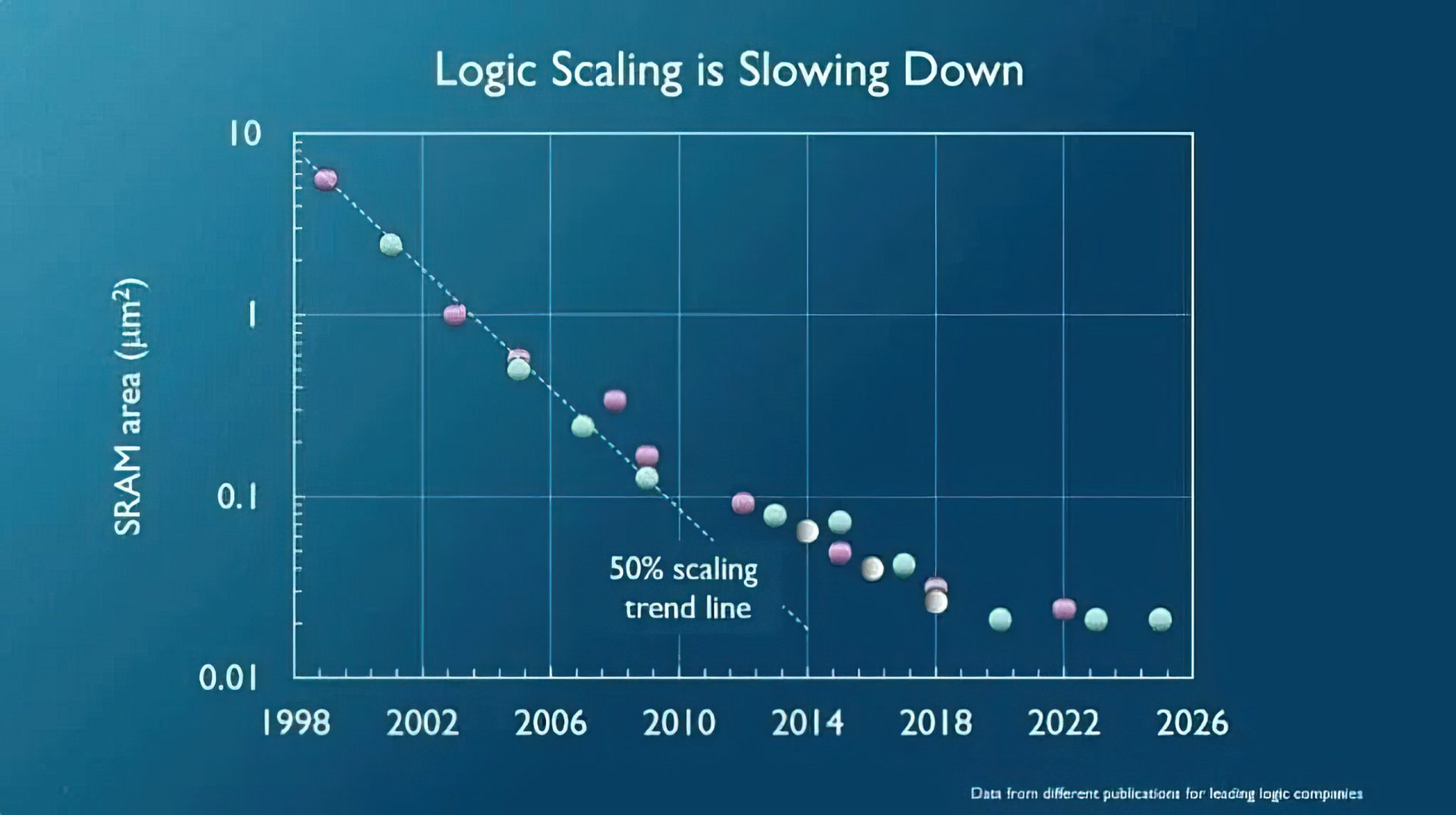
So, what’s the big idea? Traditional silicon CMOS scaling is, as the paper delicately puts it, “nearing its physical limits.” Shocker. The industry’s pivot is toward stacking transistors on top of each other, hence CFETs. But the paper’s abstract points out the current silicon-based CFETs have their own headaches: high-temperature processes that mess with underlying layers, atoms deciding to wander where they shouldn’t (dopant diffusion, for the uninitiated), and the general nightmare of getting everything lined up perfectly. It’s enough to make an engineer reach for the nearest bottle of aspirin.
The Allure of the Atomically Thin
This is where the fancy-sounding “2D materials” come in. Think graphene, but for logic gates. These materials are, by definition, incredibly thin – just one or a few atoms thick. Their theoretical advantages are numerous, and if you believe the hype, they’re practically tailor-made for this M3D world. They boast “strong electrostatics” (whatever that means in practice) and can be processed at much lower temperatures. This last point is key; it means they can theoretically be integrated without trashing the delicate circuits already built below them, a crucial requirement for the so-called back-end-of-line (BEOL) integration. The researchers even float the idea of them replacing traditional front-end-of-line (FEOL) components down the road. That’s a big leap from theoretical promise to practical application, but hey, it’s a research paper.
The paper itself dives into the nitty-gritty of what needs to happen to make this a reality. We’re talking about: * Synthesis: How do you even make these 2D materials reliably and at scale? * Channel Engineering: How do you make them act as either n-type or p-type transistors? * Contacts: Getting low-resistance connections is always a headache. * Dielectrics: Insulators are vital; getting good ones integrated is paramount. * Compatibility: Making sure these new materials play nice with existing BEOL/FEOL processes and the interconnects that glue everything together.
This isn’t just some theoretical musing. The researchers claim to have compared the thermal dissipation and energy consumption of silicon CFETs versus their 2D counterparts across different stacking configurations. Their prediction? 2D materials offer “superior thermal and power-efficiency benefits.” If that holds up, and if they can solve all the other problems, we’re looking at a pathway to what they’re calling the “Ångström-era logic architecture.” It sounds impressive, but as always, the devil is in the details – and the manufacturing costs.
Who Actually Benefits Here?
This is where my inner cynic wakes up. Everyone talks about benefits for consumers – smaller, faster devices. Sure. But who’s making money from this research now? It’s the universities, the research institutions, and likely the companies that fund them, hoping for the next big patent. The path from a lab bench discovery to a chip in your phone is a long, expensive, and often brutal one. Every few years, a new material or architecture gets touted as the next silicon killer, only to fade into obscurity because it’s too expensive, too difficult to manufacture at scale, or simply doesn’t offer a compelling enough advantage over an incrementally improved incumbent.
My unique insight here? We’ve seen this play out before. Remember when carbon nanotubes or nanowires were going to revolutionize computing? They offered incredible theoretical advantages, but manufacturing them consistently and integrating them into existing fabrication flows proved to be a monumental hurdle. 2D materials, while perhaps more amenable to some existing processes, face similar existential questions. The real question isn’t if they can be made to work in a lab, but if they can be made to work profitably in a foundry.
“While silicon (Si)-CFETs demonstrate the viability of monolithic stacking, their scalability is constrained by high thermal budgets, dopant diffusion, and alignment complexity.”
That quote alone tells you the problem they’re trying to solve. Silicon isn’t perfect. But it’s also the most mature, most understood, and most cost-effective semiconductor manufacturing process on the planet. Until 2D materials can demonstrably beat silicon on performance and cost at mass production levels, they’ll remain an interesting academic exercise, not a market disruptor. The push for Ångström-scale logic is inevitable, but the path there is littered with good intentions and failed revolutionary materials. Let’s just say I’ll be keeping a healthy dose of skepticism handy.
Is This the End of Silicon As We Know It?
Not tomorrow, and probably not next year. Silicon is incredibly resilient. It’s got decades of infrastructure, optimization, and talent built around it. What this research signifies is that the industry is looking for alternatives, and 2D materials are a serious contender in that exploration. The paper highlights potential advantages in power efficiency and thermal management, areas where silicon is starting to show its age, especially in high-performance computing and AI accelerators. If 2D materials can indeed be integrated into CFET architectures without prohibitive cost increases, they could become a complementary technology, used in specific applications where their benefits are most pronounced, rather than a wholesale replacement. Think niche applications first, broad adoption later – if ever.
Why Does This Matter for Chip Designers?
For chip designers, this research is like getting a glimpse of a possible future blueprint. If 2D materials become viable for CFETs, it opens up new design possibilities. Imagine chips that run cooler, allowing for higher clock speeds or denser integration without melting. Designers might be able to experiment with novel transistor structures and circuit layouts that simply aren’t feasible with silicon’s inherent limitations. However, it also means learning a whole new set of design rules, understanding new material properties, and grappling with new fabrication challenges. It’s exciting for innovation, but also a significant learning curve and a risk for product roadmaps.
What the Future Holds (Probably)
We’re likely a good decade or more away from seeing 2D material CFETs in your everyday devices. There are too many engineering and economic hurdles to clear. But this research pushes the envelope, forcing us to consider materials beyond silicon for the next generation of computing. It’s a marathon, not a sprint, and the finish line just got a little more interesting – and a lot more complicated.
🧬 Related Insights
- Read more: Broken RTX 5090s for AI Pros: A Half-Price Gamble
- Read more: cuTile BASIC: NVIDIA Makes GPUs Speak 1970s Code – And It Runs Lightning Fast
Frequently Asked Questions
What exactly are 2D materials in this context? 2D materials are materials that are only one or a few atoms thick, such as graphene. In this paper, they are being explored as potential replacements for silicon channels in advanced transistor designs called complementary field-effect transistors (CFETs).
Will this make my phone run faster? Potentially, in the long term. The research suggests 2D materials in CFETs could lead to more power-efficient and cooler-running chips, which could enable faster performance or longer battery life in future devices. However, widespread adoption is still many years away.
What are the main challenges for 2D CFETs? The paper outlines several challenges, including reliable synthesis of 2D materials, engineering them for specific electrical properties (n-type or p-type), creating low-resistance electrical contacts, integrating suitable gate dielectrics, and ensuring compatibility with existing manufacturing processes.