![Siemens & TSMC: AI Ignites Chip Design [Full Breakdown] — Chip Beat](/og-image.svg)
So, here’s the thing: for ages, chip design has felt like trying to build a skyscraper with tweezers. You’ve got these incredibly complex tasks – verifying every tiny transistor, ensuring signals don’t interfere, even managing the heat generated by billions of components – and they all require painstaking, human-driven effort. We’ve been inching forward, process node by process node, with incremental improvements. Everyone expected more of the same: slightly faster tools, slightly better yields, the usual slow march of technological progress.
But this Siemens and TSMC collaboration? It’s not an incremental step. This feels like we’ve just discovered gravity. They’re not just updating their existing toolchains; they’re fundamentally re-architecting the engine of IC creation with artificial intelligence. Think of it like moving from hand-cranked cars to autonomous vehicles, but for the very blueprints of our digital world. This is about taking those multi-step, multi-tool automations that used to take weeks and compressing them into hours, maybe even minutes.
Is This Just More Corporate Buzz? How AI Changes the Game
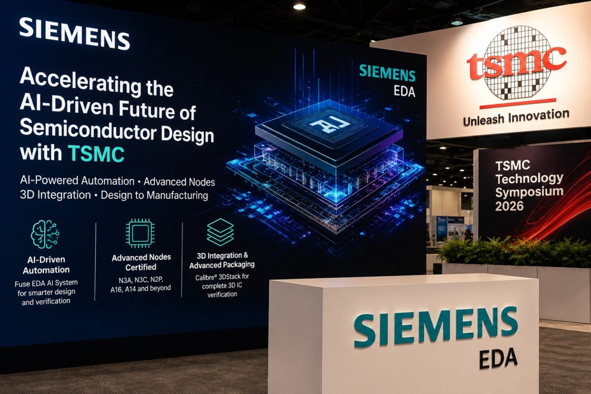
Look, I’m as skeptical as the next journalist when I hear terms like “AI-enhanced.” Usually, it’s just a shiny coat of paint on old software. But here, the implications are seismic. Siemens’ Calibre software, the gold standard for physical verification, is now deeply intertwined with AI. This isn’t just about catching bugs; it’s about predicting them, guiding designers with real-time recommendations, and executing complex commands faster than a human eye can follow. It’s like having a legion of infinitely patient, hyper-intelligent interns working on your most critical design challenges.
And this isn’t just for the bleeding edge either. TSMC’s 3DFabric technologies, which are all about stacking chips vertically like a futuristic digital city, are getting an AI boost. Calibre 3DStack is now handling interface checks, 3D-aware DRC validation, and even thermal analysis with AI. Imagine trying to manage the heat generated by multiple stacked chips without AI – it’s a nightmare. Now, designers can get real-time thermal insights, crucial for making informed decisions about how these dense, 3D-stacked systems will actually perform.
Siemens’ Calibre nmPlatform software has achieved certification for TSMC’s 3nm, 2nm, A16 and A14 process technologies. This collaboration expands into TSMC’s custom design reference flow (CDRF) on its A14 process, where Siemens’ Solido Simulation Suite supports reliability aware simulation technology.
This partnership is hitting every key aspect of the design cycle. From the microscopic level of transistor simulation with Solido Simulation Suite (now certified for TSMC’s advanced N3A, N2P, A16, and A14 processes) to the macroscopic view of power delivery and thermal management, AI is becoming the central nervous system. Siemens’ Aprisa software, vital for digital implementation, has also received TSMC N2P Integrated Tool Certification. This means it’s ready to handle the immense complexity of designing at these advanced nodes, all powered by AI-driven optimizations.
Why Does This Matter for the Future of Chips?
My unique insight here? This isn’t just about speeding up current designs. This is about unlocking entirely new design paradigms. When you remove the brute-force human labor from verification and simulation, you free up designers to explore more radical architectures. We’re talking about more complex multi-chiplet designs, more innovative packaging solutions, and even advancements in areas like silicon photonics (which Siemens’ Innovator3D IC software is now directly supporting for TSMC-COUPE technology). The bottleneck has always been human capacity to verify complexity. AI smashes that bottleneck.
Think of it as AI not as a tool, but as a fundamental platform shift, much like the internet or the smartphone. It’s changing the very grammar of how we create technology. The days of incremental improvements are over. We’re entering an era where AI actively participates in the discovery of better chip designs. This means we can expect not just faster chips, but chips that are more power-efficient, more integrated, and capable of handling the exponentially growing demands of AI itself.
This collaboration is a clear signal: the future of chip design is not just about smaller transistors; it’s about smarter processes. It’s about using AI to amplify human ingenuity to an unprecedented degree. And for us as consumers, and for the industries that rely on advanced silicon, that means a future brimming with more powerful, more capable, and more innovative technology than we could have imagined even a few years ago.
🧬 Related Insights
- Read more: Google Splits TPUs: Training vs Inference [Cloud Next ‘26]
- Read more: Ajinomoto’s ABF Shortage Could Delay NVIDIA’s Next AI Chip Wave by Months
Frequently Asked Questions
What does Siemens’ Calibre software do? Siemens’ Calibre is a suite of tools used in semiconductor manufacturing for verifying that chip designs meet the strict physical and electrical rules required for fabrication. It’s like the ultimate quality control inspector for the tiny blueprints of computer chips.
How does AI help TSMC design chips? AI is being integrated into TSMC’s design workflows to automate complex verification tasks, predict design issues before they occur, and provide real-time guidance to designers. This speeds up the design cycle and allows for the creation of more complex and efficient chips.
Will this collaboration make chips cheaper? While the immediate focus is on enabling more complex designs and accelerating development, the long-term impact of AI-driven efficiency in chip design could lead to reduced development costs and potentially more affordable, advanced chips. However, the initial investment in these advanced processes and tools is substantial.