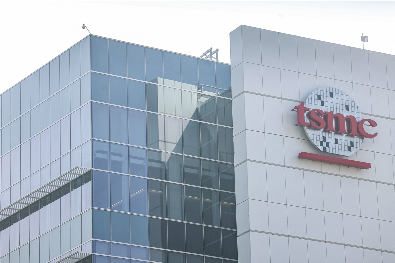
So, Applied Materials and TSMC, two titans of the chip world, are buddying up. Big news, right? They’re going to be co-innovating at Applied’s shiny new $5 billion EPIC Center in Silicon Valley. Their stated goal? To push the boundaries of materials engineering and equipment to build the semiconductors we’ll need for the “next era of AI.” Sounds impressive. Another glossy press release, another partnership announcement designed to make investors feel warm and fuzzy about the future of silicon. But let’s pump the brakes for a second.
For two decades, I’ve watched these companies announce partnerships, open new facilities, and promise the moon. The sheer volume of these announcements can be deafening, often obscuring the fundamental question: who is actually making the money here, and how much? Applied, the equipment giant, needs TSMC, the world’s dominant foundry, to buy their machines and use their materials. TSMC needs Applied’s bleeding-edge tech to stay ahead of the curve and, more importantly, to meet the insatiable demand for more powerful, more efficient chips – particularly the ones powering AI.
This partnership at the EPIC Center is presented as an acceleration of the innovation pipeline. Dr. Y.J. Mii, TSMC’s EVP, stated, “Meeting the challenges of AI at a global scale requires industry-wide collaboration.” Sure. And Gary Dickerson, Applied’s CEO, chimed in that they’re “strengthening that partnership and accelerating the development of technologies to address the unprecedented complexity driving the chipmaking roadmap.” It’s the standard playbook: praise the partner, highlight the complexity, and promise acceleration. But what does that acceleration really mean in practice?
It means TSMC gets earlier access to Applied’s R&D. It means they can test out new materials and equipment designed for complex 3D transistor structures and advanced interconnects before they’re pushed into mass production. The EPIC Center, according to Applied, is designed to “dramatically reduce the time it takes to commercialize breakthrough technologies.” This is where the skepticism kicks in. We’re talking about the most complex manufacturing process on Earth. “Reducing time” in this context might mean shaving a few months off a multi-year development cycle, not suddenly churning out revolutionary chips overnight.
The Real Business of Co-Innovation
Let’s be blunt: this is about securing future revenue streams. Applied Materials makes money by selling incredibly expensive, highly specialized manufacturing equipment. TSMC makes money by manufacturing chips for everyone else. The more advanced and difficult the chips become – and AI chips are very difficult – the more critical their manufacturing process, and thus the more essential the equipment suppliers like Applied become. It’s a symbiotic relationship, but it’s also a high-stakes arms race.
Think about it. The demands on materials engineering are escalating. New architectures mean new materials, new ways of depositing and etching them, and new equipment to handle it all with sub-atomic precision. Applied’s $5 billion EPIC Center is a massive investment. They need to demonstrate that this investment translates into tangible benefits for their customers, like TSMC. This partnership is a PR win for Applied, showcasing their commitment to the leading edge, and a strategic move for TSMC, ensuring they have a dedicated pipeline of advanced manufacturing solutions.
“As semiconductor device architectures evolve with each new generation, the demands on materials engineering and process integration continue to increase,” said Dr. Y.J. Mii, Executive Vice President and Co-Chief Operating Officer at TSMC. “Meeting the challenges of AI at a global scale requires industry-wide collaboration.”
Is this a genuine, disruptive leap forward? Or is it more like two companies polishing the same old engine while shouting about how fast they’re going to go? The real test will be in the silicon that rolls off TSMC’s lines and the profit margins Applied Materials reports in the coming years. Until then, it’s a carefully crafted narrative about collaboration and future-proofing.
Why Does This Matter for AI Development?
The push for more powerful AI isn’t slowing down. It’s accelerating. This means chips need to be faster, more energy-efficient, and capable of handling massive datasets. Traditional scaling methods are hitting their limits. So, we’re seeing a shift towards novel materials, complex 3D architectures (like stacked transistors and interconnects), and complex process integration. Applied Materials is positioning itself as the indispensable partner in this transition. By working hand-in-hand with TSMC, they can tailor their equipment and materials precisely to the needs of next-generation chip designs, hopefully bypassing some of the traditional development hurdles.
For developers and end-users, the implication is simple: more powerful AI tools and applications are on the horizon. This collaboration could lead to more capable AI models running on more efficient hardware, potentially reducing energy consumption and increasing processing speeds. It’s about building the foundational infrastructure for tomorrow’s AI breakthroughs, even if the pronouncements from the C-suites sound like standard corporate fare.
Ultimately, this partnership highlights the intense competition and massive investment fueling the AI chip race. It’s not just about chip design anymore; it’s about the complex, often unglamorous, but absolutely critical manufacturing processes that bring those designs to life. Applied Materials and TSMC are making a bold statement by pooling their resources at the EPIC Center, but the proof will be in the performance and accessibility of the AI chips they help create.
🧬 Related Insights
- Read more: Apple’s Memory Grab: Chinese Flagships Face Extinction
- Read more: Qualcomm Defends Samsung Share Amid Exynos Push [70%+]
Frequently Asked Questions
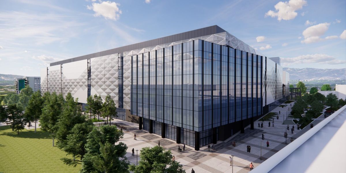
What is the EPIC Center? The EPIC Center is Applied Materials’ new, $5 billion research and development facility in Silicon Valley, designed to accelerate the development and commercialization of advanced semiconductor manufacturing technologies.
How will this partnership accelerate AI scaling? By co-innovating at the EPIC Center, Applied Materials and TSMC aim to speed up advancements in materials engineering, equipment, and process integration needed for next-generation AI chips, potentially reducing the time from research to high-volume manufacturing.
Will this partnership lead to cheaper AI chips? While the partnership aims to improve efficiency and performance, its primary focus is on enabling more advanced chip architectures. Any impact on chip cost will depend on numerous factors beyond this collaboration, including market demand and manufacturing yields.