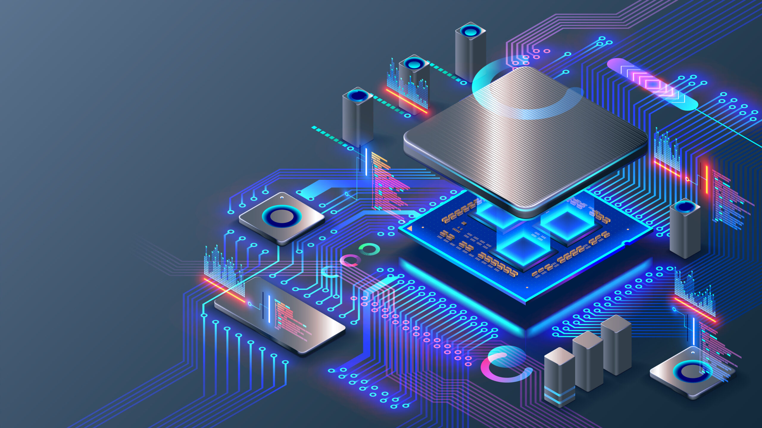
Look, we’re on the cusp of something truly wild. Forget those monolithic slabs of silicon we’ve been cramming every function into for decades. The future of computing is about to get modular, stacked, and unbelievably powerful. Think of it like Lego for silicon, where specialized ‘chiplets’ snap together to create a super-brain. This approach promises more bang for your buck – faster processors, more memory, specialized AI accelerators, all in one tightly integrated package. It’s the kind of architectural leap that makes your Jaw. Drop.
But here’s the rub, and it’s a big one. As we start stacking these delicate little silicon brains on top of each other, we’re opening them up to a hidden, invisible menace: electrostatic discharge, or ESD. You know that little shock you get when you touch a doorknob after walking across carpet? That’s ESD. For our everyday electronics, it’s usually just a minor annoyance. For the hyper-sensitive, interconnected chiplets of tomorrow, it’s potentially catastrophic. A single errant zap could ripple through the entire system, bricking your next-gen device before it even gets out of the box.
This isn’t some far-off sci-fi problem. Researchers at the University of California, Riverside, are already sounding the alarm in their latest paper, aptly titled ‘In-SoIC ESD Protection for Chiplet-Based 3D Microsystems: Future Research Directions.’ They’re not just talking about a niche engineering headache; they’re pinpointing a fundamental roadblock for the entire chiplet revolution. If we can’t reliably protect these interconnected chiplets from static electricity, all that promise of unprecedented performance and functionality could fizzle out like a cheap firework.
Why is this so tricky? Because these chiplets aren’t just sitting side-by-side; they’re often stacked vertically, with incredibly fine connections between them. Traditional ESD protection methods, which often involve beefier silicon structures on the edges of a chip, just don’t scale or fit neatly into this new 3D architecture. Imagine trying to build a skyscraper with the same fire escape design as a single-story bungalow. It just won’t cut it. The very nature of heterogeneous integration – mixing and matching different types of chiplets – means we need novel, integrated ESD solutions that work across diverse materials and interconnects.
So, what does this mean for you, the person who’ll be using these incredible new machines? It means the pace of innovation, the leap in raw processing power and functionality we’ve been expecting, could be significantly slowed down if this ESD challenge isn’t met head-on. Think of it like a racehorse that’s incredibly fast but has a tendency to trip. Until we find a way to smooth out those bumps, that incredible speed remains untapped potential. It’s not just about making chips more powerful; it’s about making them reliable enough to actually use that power.
And here’s my unique take: While the UC Riverside paper focuses on the technical challenge, the real story is the invisible arms race happening behind the scenes. Companies aren’t just developing faster chips; they’re developing resilience. They’re building the invisible shields that will allow these incredible machines to survive the mundane, yet destructive, forces of our everyday world. This isn’t just about better silicon; it’s about building a foundation of trust for the next era of computing.
The paper itself is a clear call to action, stating:
Electrostatic discharge reliability is a major challenge to future smart chips featuring rich functionalities and ultra performance, utilizing advanced heterogeneous integration and packaging technologies.
It’s a stark reminder that for every leap in performance, there’s an equal and opposite need for strong engineering. The folks at UC Riverside are pointing out a critical vulnerability, a potential Achilles’ heel for the chiplet future. They’re essentially saying, ‘Hey, we’re building these amazing modular brains, but watch out for the static shocks!’
What’s fascinating is that this isn’t just an academic exercise. Major players in the semiconductor industry are undoubtedly pouring resources into solving this. The future of AI, of immersive virtual worlds, of personalized medicine delivered via silicon – all of it hinges on overcoming these fundamental protection issues. It’s the unsung hero of technological progress: the painstaking work to make the futuristic work.
This research points towards a future where ESD protection isn’t an afterthought, but an integral part of the chiplet design itself. It’s like building the foundations of your house specifically to withstand earthquakes, rather than just slapping on some paint and hoping for the best. We’re talking about tiny, hyper-efficient protection circuits woven into the very fabric of these stacked chips. It’s complex, it’s challenging, and it’s absolutely essential for the continued exponential growth of computing.
The Chiplet Stack and the Sparky Threat
For years, we’ve been cramming more and more transistors onto single chips. But physics is a harsh mistress, and we’re hitting limits. Chiplets are the elegant workaround – smaller, specialized chips that work together. Imagine a smartphone where the CPU, GPU, AI processor, and memory are all separate, perfectly tuned modules that communicate at light speed. That’s the chiplet dream. It allows for incredible customization and performance scaling. But in a 3D stack, these communication pathways are shorter, faster, and, unfortunately, more vulnerable to tiny electrical surges.
When you’re dealing with these incredibly dense, interconnected structures, a stray static charge, which might barely register on a single, strong chip, can cascade through the delicate interconnects and into sensitive components. The UC Riverside paper highlights that traditional, off-chip ESD protection isn’t sufficient for these complex 3D microsystems. We need solutions that are embedded within the chiplet architecture itself, offering protection at the most granular level. It’s a fundamental shift in how we approach reliability.
Future Research: What’s Next?
The paper outlines several promising avenues for future research, from exploring new materials with inherent ESD resistance to developing smarter, on-chip protection circuits that can dynamically sense and shunt away dangerous electrical charges. It’s a complex puzzle, and the researchers are looking for answers in areas like advanced packaging techniques and novel circuit designs. The goal is to ensure that the incredible power promised by chiplets isn’t undermined by a common, everyday electrical phenomenon. They’re not just identifying a problem; they’re laying out the roadmap to solve it, ensuring that the future of computing is not only powerful but also resilient.
Will this sparky problem slow down my next computer?
Potentially, yes. If strong ESD protection solutions for chiplets aren’t developed and implemented effectively, it could delay the widespread adoption of the most advanced chiplet designs. This might mean a slower-than-expected increase in raw performance for consumer devices and high-performance computing. Think of it as a bottleneck – the processing power is there, but the ability to reliably deliver it is being held up.
What are chiplets exactly?
Chiplets are essentially smaller, specialized semiconductor dies that are designed to work together as a single system. Instead of building one massive, complex chip with all functions, designers can combine multiple smaller, optimized chiplets (like a CPU chiplet, a GPU chiplet, and a memory chiplet) to create a powerful and flexible system. This is a key trend in modern chip design, allowing for more tailored and cost-effective solutions.
How is this different from older chip protection?
Older chips often relied on larger, more strong designs and off-chip protection circuits. With chiplets, especially in 3D stacked configurations, the interconnects are much finer and closer. This means that ESD events can propagate more easily and cause damage to adjacent chiplets. Therefore, new, more integrated, and highly localized protection mechanisms are needed, woven directly into the chiplet design itself, rather than relying solely on external safeguards.