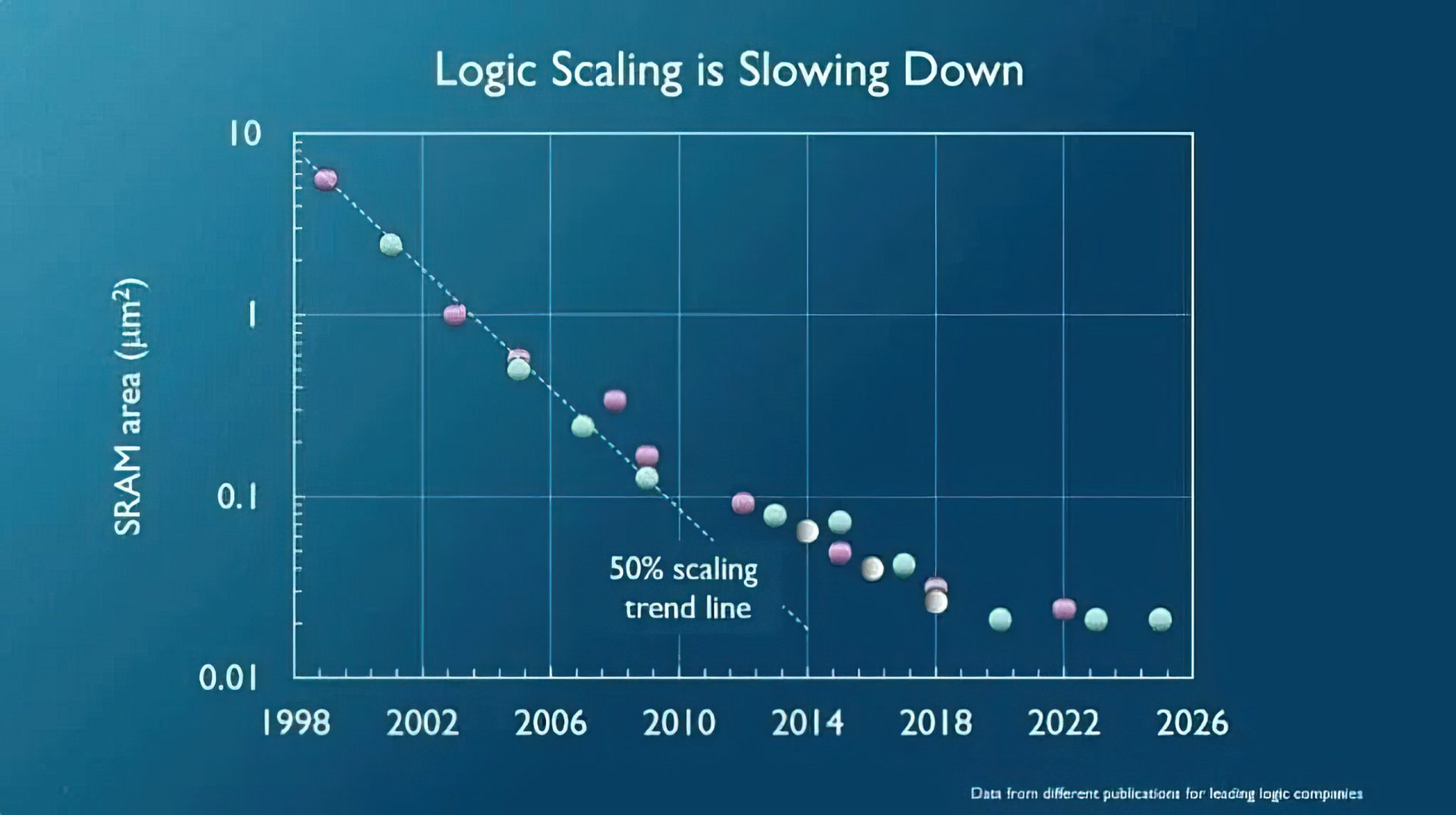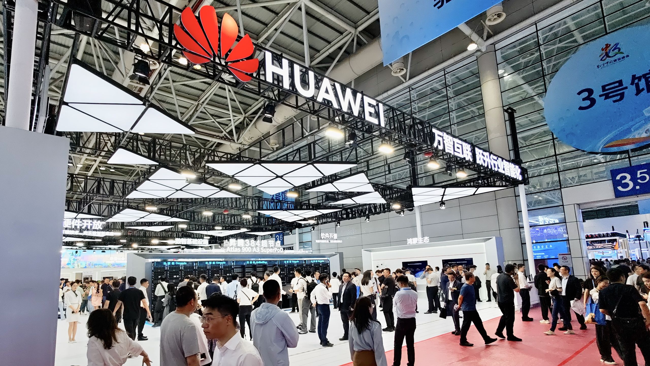
Forget brute-force transistor shrinking. Huawei, facing the undeniable wall of Moore’s Law’s diminishing returns, is charting a course less traveled. Their latest semiconductor roadmap ditches the singular pursuit of smaller nodes, opting instead for a holistic approach: architecture, interconnects, and system-level optimizations designed to deliver 1.4nm-equivalent performance. It’s a strategic pivot that acknowledges the physics but refuses to accept the limitations.
Here’s the thing: the industry has been talking about this for years. Analysts have pointed to advanced packaging, specialized accelerators, and software co-design as the next frontiers. But Huawei’s announcement isn’t just talk; it’s a concrete, albeit high-level, strategy document. They’re not waiting for the next lithography breakthrough, they’re building it with existing and near-future tools, just applied with a different philosophy.
The Limits of ‘Shrink First’
The relentless march of Moore’s Law—the observation that the number of transistors on a microchip doubles roughly every two years—has defined semiconductor progress for decades. Yet, the economic and physical barriers to continued shrinking are now starkly apparent. Each new node generation demands astronomical R&D and manufacturing investments, with diminishing performance gains. This is where Huawei’s strategy deviates sharply. Instead of solely pushing for smaller, denser transistors, they’re looking at how to make the entire system smarter.
Consider the implications. While TSMC and Intel wrestle with the physics of EUV lithography at 3nm and below, Huawei is signaling a move towards a performance ceiling achievable through innovation elsewhere. This means an increased emphasis on how different components communicate, how software interacts with hardware, and novel chip architectures that can perform tasks more efficiently, even if the individual transistors aren’t microscopically smaller. It’s a bit like getting a sports car to go faster not just by making the engine bigger, but by improving the aerodynamics, suspension, and transmission.
Is This a Real Threat to Global Chip Leaders?
This is the million-dollar question, isn’t it? For years, Huawei’s chip ambitions have been constrained by U.S. sanctions, effectively hobbling their access to cutting-edge manufacturing. However, this roadmap suggests a determination to overcome those hurdles through sheer engineering ingenuity. They aim to achieve what would typically require a 1.4nm process node through these alternative means. If successful, even with domestic manufacturing limitations, it signifies a formidable ability to innovate and extract performance. This could mean their chips, even if manufactured on older nodes, perform comparably in specific workloads to those made by global leaders on the latest processes.
“Our roadmap is to achieve 1.4nm-equivalent performance through architecture, interconnect, and system-level optimization, rather than solely relying on transistor scaling.” This quote, likely from an internal Huawei briefing, underlines a commitment to an alternative path.
This isn’t just about catching up; it’s about redefining the race. The traditional metrics of transistor density will likely remain important for some applications, but Huawei’s focus suggests a future where system-level intelligence and specialized architectures are paramount. This could be particularly impactful in areas like AI and high-performance computing, where efficient data movement and parallel processing are key.
What does this mean for the established giants? It forces a re-evaluation of their own roadmaps. While they continue to invest billions in shrinking transistors, they may need to allocate more resources towards inter-chip communication technologies, advanced packaging (like chiplets), and deeper software-hardware co-design to compete with an increasingly innovative Huawei. It’s a competitive pressure cooker, and Huawei just turned up the heat.
🧬 Related Insights
- Read more: SNIA’s MRAM Alliance SIG: Ecosystem Push or Hype? [2026]
- Read more: AI is the New Electricity: Samsung TV Boxes & Celebrity Rights
Frequently Asked Questions
What is Huawei’s new semiconductor roadmap targeting? Huawei’s new roadmap aims to achieve 1.4nm-equivalent chip performance by focusing on architectural improvements, advanced interconnects, and system-level optimizations, rather than relying solely on shrinking transistor sizes.
Will Huawei’s strategy bypass traditional semiconductor manufacturing limits? Yes, the strategy is designed to circumvent the traditional limits of Moore’s Law by achieving comparable performance through smarter design and system integration, rather than requiring the most advanced and costly lithography processes.
How does this differ from typical chip development? Traditionally, chip development heavily relied on transistor scaling (Moore’s Law). Huawei’s approach shifts emphasis to optimizing the overall system—how chips communicate, how they’re designed architecturally, and how software utilizes them—to achieve performance gains.