Everyone figured HBM4 would be another spec sheet dream, right? You know the drill: memory vendors promise terabytes-per-second bandwidth, AI chip designers salivate, then reality hits with signal mush at high speeds. Synopsys upended that script this week. Their test chip — world’s first HBM4 IP in silicon — actually talked to real HBM4 DRAMs, eyes wide open at 9.2 Gbps. Early HBM4 validation isn’t just PR fluff; it’s the system-level proof that next-gen AI and HPC won’t choke on memory lanes.
Look, I’ve covered memory wars since HBM2 was the hot new thing back in 2013. Back then, Nvidia’s P100 GPUs needed it to train deep nets without dying of thirst. Fast-forward — or not so fast — and here we are, with HBM4 facing the same old demons: crosstalk, power noise, package losses in those fancy multi-die setups. But Synopsys didn’t stop at ‘first silicon.’ They validated the full chain: controller, PHY, interposer, memory dice. That’s the game-changer.
Why Bother with Early HBM4 Validation?
Because late discoveries kill schedules. Imagine pouring billions into a 2nm AI superchip, only to find your HBM4 interface looks like a drunkard’s scribble under the scope. Multi-die designs? Lead times stretch years. Packaging choices lock in early. One glitch, and you’re redesigning — costly as hell.
Synopsys’ demo shows clean eyes at max DRAM rates today, with headroom for faster as memory catches up. It’s not hype; it’s silicon talking.
First silicon alone is no longer sufficient to establish readiness for next-generation designs.
That’s straight from the industry playbook now. And Synopsys lived it.
Here’s the cynical bit — my unique scoop after two decades watching Valley grifts. This reeks of the HBM3 rollout in 2022, when Micron and Samsung trash-talked yields while Synopsys and Cadence raced to certify PHYs. Back then, first-gen HBM3 chips flopped in real systems due to unvalidated paths. Synopsys learned: bake in ecosystem tests early. Prediction? They’ll lock 60% HBM4 IP market share by 2026, squeezing rivals like Alphawave. Who’s making money? Not the hyperscalers buying the systems — it’s IP houses and OSATs like TSMC’s CoWoS partners.
But — and it’s a big but — 9.2 Gbps per pin? HBM4’s specced wider, up to 16-high stacks. Bandwidth math: previous HBM3E hit 1.2 TB/s per stack. HBM4? Promises 2+ TB/s. Fine, but power. These stacks guzzle juice, and AI racks already melt data centers. Synopsys skirts that, focusing on signals. Smart PR spin — they control the PHY, not the DRAM power hogs.
Is Synopsys’ HBM4 Test Chip a Big Deal for AI Chips?
Short answer: Yes, for Nvidia, AMD, anyone chasing Blackwell or MI300 successors. Those beasts cram dies like sardines, needing bandwidth that DDR5 can’t touch. HBM4 validation de-risks tapeouts. System architects sleep better knowing the chain holds at speed.
Dig deeper. Dense interconnects mean crosstalk nightmares. Timing jitter from power noise. Channel losses in silicon interposers. Synopsys measured eyes — those oscilloscope beauties showing signal windows — and they popped at full tilt. No squint required.
In the Synopsys test chip, eye measurements demonstrate reliable operation at 9.2 Gbps, corresponding to the maximum data rate supported by the integrated HBM4 DRAMs.
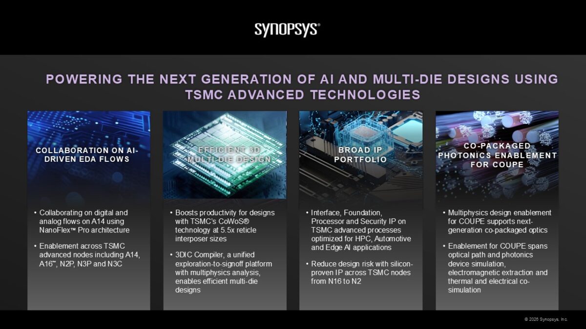
Ecosystem alignment’s the real win. Memory giants (Samsung, SK Hynix, Micron) supplied DRAMs. Foundries nodded. Packaging houses tuned interposers. This isn’t solo; it’s a convoy forming.
Skeptical lens: Synopsys’ blog screams ‘leadership’ — classic vendor chest-thump. But silicon doesn’t lie. Unlike spec sheets.
Now, the money question. Hyperscalers like Google, Meta? They’re bandwidth starved, training GPT-5 scale models. HBM4 could double throughput, slash training time. But costs? Stacks pricier than HBM3 by 50%. Who’s paying? Cloud giants, passing it to you via higher API bills.
And power efficiency — the elephant. HBM4 pushes voltages tight, but noise floors rise. If it doesn’t beat HBM3E pJ/bit, it’s dead on arrival for edge HPC. My bet: it’ll shine in fat-server AI, flop in mobile.
What About HPC and the Bigger Picture?
HPC’s bandwidth junkie too. Frontier, Aurora supercomputers lap up HBM3. Next Frontier? HBM4 or bust for exascale-plus. Early validation speeds that.
Industry ripple: Cadence, Alphawave scrambling. Memory vendors ramp silicon. TSMC/Intel foundries tweak processes. It’s a feeding frenzy.
One para wonder: Risks drop, tapeouts accelerate, AI arms race heats up.
But here’s the veteran gut-check. Remember GDDR6X hype for RTX 30? Bandwidth bonanza, then thermal walls. HBM4 risks same if packaging lags. Synopsys advances the ball, but ecosystem must score.
Bold call: By 2025, HBM4 powers 80% of >100kW AI accelerators. Synopsys royalties flow like champagne.
Wrapping the cynicism — this milestone’s legit, cuts through buzzword fog. AI/HPC marches on, fatter pipes ahead. Just watch the power bills.
🧬 Related Insights
- Read more: Aparna Bawa Jumps from Zoom to Intel: The Culture Fixer Chipmakers Desperately Need
- Read more: SK Hynix’s Photolithography ‘Master Key’ Cracks Open AI Memory Scaling Limits
Frequently Asked Questions
What is HBM4 and why does it matter for AI?
HBM4 stacks DRAM vertically for insane bandwidth — think 2 TB/s per stack — crucial for training massive LLMs without memory bottlenecks.
Does Synopsys HBM4 validation mean next-gen GPUs are imminent?
It de-risks designs, so yes — Nvidia/AMD tapeouts safer, but full chips still 12-18 months out.
Will HBM4 solve AI data center power problems?
Bandwidth yes, power no — expect hotter racks unless efficiency jumps.