A laser pulse, invisible and merciless, carves patterns a few nanometers wide onto a spinning silicon wafer in SK Hynix’s Icheon fab—precision that turns raw sand into the lifeblood of AI superclusters.
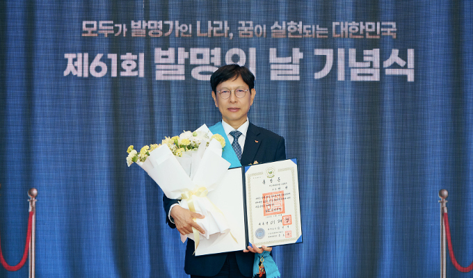
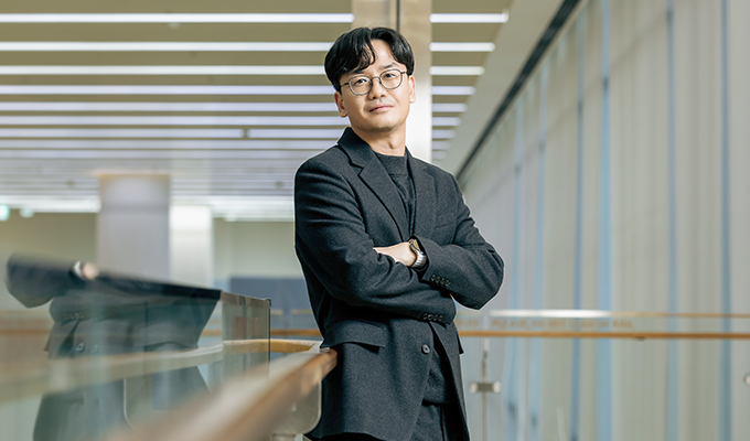
SK Hynix photolithography doesn’t grab headlines like HBM stacks or Nvidia deals, but it’s the hidden engine driving the company’s AI memory surge. VP Hyunsok Kim, freshly minted head of Photo Technology, frames it as the ‘scaling master key’—a tool to etch ever-tinier, ever-more-complex circuits without yields cratering. And here’s the thing: in an era where AI demands denser, faster memory, this isn’t hype. It’s architecture.
Kim’s been at it since 2004, chasing that engineer’s high from impossible feats. Now? Responsibility weighs heavier than any reticle.
The Weight of the Wafer
He’s not mincing words about the shift. From solo pattern-pushing to department steering, Kim sees photolithography as SK Hynix’s linchpin against Samsung and Micron.
“I’m honored to take on such an important role at this vital juncture in the AI transformation, but I also feel a profound sense of responsibility,” Kim shared. “Moving beyond my past role as an engineer, I now stand at a new starting point where I must consider the broader direction and mission of the entire organization. As a leader who sees not just the trees but the entire forest, I pledge to guide the Photo Technology department forward.”
That forest? It’s tangled with EUV challenges—extreme ultraviolet light bending physics to print features at 1c DRAM scales. Kim’s team nailed process stability last year, a quiet win that greased HBM ramps and shaved months off roadmaps.
But why does this matter? Scaling’s hitting walls—quantum tunneling, line-edge roughness—and EUV’s the hammer. Stabilize it, and you own cost curves. Botch it, and your multi-billion fab sits idle.
Short paragraphs like this one hit hard. Then sprawl: Kim’s pushing a ‘smart, data-driven’ lithography pipeline, feeding sensor data from exposure tools into AI models that predict defects before they print. It’s not magic—it’s feedback loops honed over decades, now supercharged for custom AI memory flavors. (Samsung’s chasing similar, but SK Hynix’s HBM edge gives them pole position.)
Why Is EUV Stability SK Hynix’s Secret Weapon?
EUV lithography—ASML’s monopoly jewel—demands vacuum chambers, plasma sources spitting 13.5nm light, and mirrors polished to atomic flatness. One wobble in dose or focus? Yields tank 20%. Kim’s crew fixed that.
“Recently, the Photo Technology department made a significant improvement in EUV process stability, enabling the successful development of 1c DRAM and contributing to the timely development of High-Bandwidth Memory (HBM),” Kim explained.
This isn’t incremental. It’s the platform for 2026’s full-stack vision: design-to-package AI memory tailored for hyperscalers. Photolithography patterns dictate transistor density, signal integrity—everything downstream.
Look, competitors like TSMC pour billions into EUV for logic, but memory’s different. HBM stacks 12 layers high; one layer’s blur ripples through. SK Hynix’s stability? It buys time-to-market, slashes defect costs—pure competitiveness.
And.
Kim leads from the front. ‘First to lead. Last to leave.’ That’s his mantra—boots-on-wafer-floor style.
Can Photolithography Make SK Hynix Unassailable in AI Memory?
Here’s my take, absent from the press release: this ‘master key’ echoes the 1980s lithography wars, when Japanese firms like Nikon crushed U.S. incumbents by mastering steppers. Back then, it was i-line light; now EUV. SK Hynix, Korean underdog turned HBM king, could pull a repeat—locking in custom AI stacks before rivals scale.
Bold prediction: By 2027, expect SK Hynix HBM3e yields hitting 90%+ on EUV, undercutting Samsung by 15% on cost-per-bit. Why? Data-driven tweaks (machine learning on overlay errors) turn fabs into predictive beasts. Corporate spin calls it ‘profound responsibility’—fair, but it’s survival math.
Critique time. Kim’s vision sounds smoothly, yet EUV’s track record screams variability: source power fluctuations, stochastic noise at 3nm. They’ve stabilized—great—but production marathons (12 wafer-hours per lot) will test it. If yields hold under AI frenzy, game over for laggards.
The how: Overlay control to 1nm. Resist adhesion under plasma assault. Dose uniformity across 300mm wafers. Kim’s roadmap? AI-orchestrated metrology, real-time corrections—architectural shift from rule-based to probabilistic patterning.
Teams grind here. Engineers tweak pellicles at 3am. Kim stays till last.
Full-stack means owning the stack: HBM for GPUs, CXL for disagg, custom DRAM for inference. Photolithography unlocks it—translating diverse designs faithfully.
“As scaling approaches its limits, the ability to manage EUV technology efficiently and reliably will determine both product quality and cost competitiveness,” Kim emphasized.
Yes. And SK Hynix’s playing to win.
🧬 Related Insights
- Read more: NVIDIA’s GH200 Just Clocked Single-Digit Microsecond Latency in Trading – GPUs Strike Back at FPGAs
- Read more: Intel’s Innovation Engine Roars Back to Life
Frequently Asked Questions
What is SK Hynix’s ‘Scaling Master Key’?
It’s photolithography tech, led by VP Hyunsok Kim, that stabilizes EUV processes for ultra-fine AI memory patterns, boosting yields and speed-to-market.
How does EUV change HBM production?
EUV enables denser layers with better stability, cutting defects in high-bandwidth memory crucial for Nvidia’s AI GPUs—key to SK Hynix’s market lead.
Who is Hyunsok Kim at SK Hynix?
Photo Technology VP since 2024, 20-year vet pushing EUV limits for DRAM and HBM, now steering full-stack AI memory innovations.