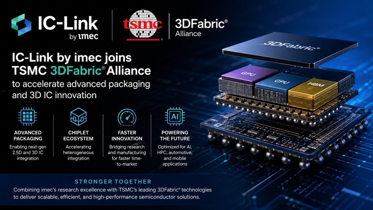
AI Design Alliance Gets Serious.
The chip design software giant Synopsys, and TSMC, the world’s leading contract chip manufacturer, have just announced a significant ramp-up of their partnership. This isn’t just another drip-feed of R&D updates; it’s a strategic acceleration aimed squarely at the AI hardware gold rush, promising to bake cutting-edge silicon IP, AI-infused design tools, and TSMC’s most advanced manufacturing processes into a single, tightly coupled offering. The goal? To slash the time it takes to bring high-performance computing and AI systems from concept to silicon. Think of it as an industrial-scale upgrade for how AI chips are conceived and built.
What’s Under the Hood?
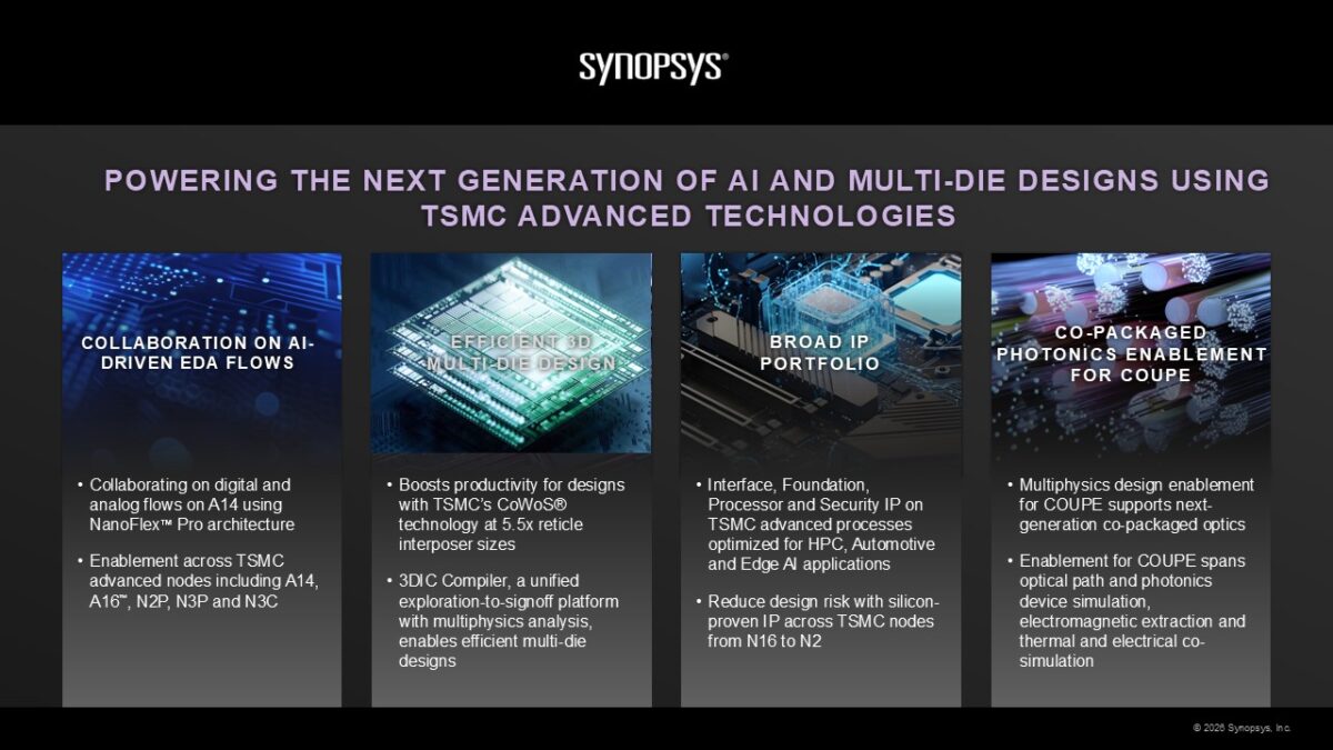
This expansion isn’t monolithic; it’s a three-pronged assault on design bottlenecks. First, Synopsys is pushing its silicon-proven interface IP onto TSMC’s bleeding-edge process nodes, including the now-in-vogue 3nm and the even more elusive 2nm. We’re talking about next-gen standards like M-PHY v6.0, which is apparently already seeing low-power silicon bring-up on TSMC’s N2P process, and tapeouts for 64G UCIe IP and 224G high-speed interconnects. For AI chips, which are essentially massive data-moving engines, this is the plumbing that keeps the whole operation from drowning in its own information.
Then there’s the EDA (Electronic Design Automation) piece. The collaboration is beefing up certified design flows, and the key here is an increased emphasis on agentic AI-driven optimization. This means Synopsys Fusion Compiler, working with TSMC’s A14 process and NanoFlex Pro architecture, is moving beyond mere assistance to actively guiding design decisions to wring out better power, performance, and area (PPA). It’s a subtle but critical shift from AI as a helpful intern to AI as a lead engineer, capable of making complex, impactful calls.
Beyond the individual chip, the partnership is also targeting system-level integration and advanced packaging. Synopsys’ 3DIC Compiler platform is now designed to boost productivity for TSMC’s CoWoS technology, handling interposer sizes up to a staggering 5.5 times the reticle limit. That’s a clear nod to the reality of modern, multi-die designs where stitching together multiple specialized chips is the new norm. And to ensure these complex systems don’t overheat or electrocute themselves, they’re enhancing multiphysics simulation capabilities to account for thermal, electrical, and optical interactions.
Targeting New Frontiers
The reach of this alliance extends beyond the usual hyperscale data centers. In the automotive sector, Synopsys is rolling out a UCIe IP solution compliant with ASIL B functional safety requirements on TSMC’s N5A process. This is a big deal for safety-critical applications, making chiplet architectures a more viable, and verifiable, option. For mobile and storage, advancements in M-PHY IP are geared towards smartphones and storage devices that are increasingly demanding both raw power and ironclad power efficiency.
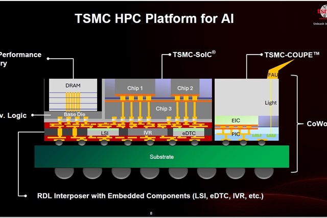
And to power the very AI infrastructure that runs everything else, the collaboration is diving headfirst into co-packaged optics. This involves co-design enablement for optical systems, including TSMC’s COUPE design flow, and pairing it with 224G IP. The aim is to tackle the escalating bandwidth and energy demands that threaten to choke large-scale AI deployments. It’s about ensuring the data can get where it needs to go, fast and without breaking the bank on electricity.
Why Does This Matter for AI Hardware?
The core problem in AI hardware today isn’t just raw compute power; it’s the plumbing. As processors get faster, the real bottlenecks have become data movement, power consumption, and the sheer complexity of putting it all together. By unifying high-speed IP, intelligent design tools, and advanced manufacturing, Synopsys and TSMC are creating a more direct path from a complex design spec to a manufacturable chip. This is precisely the kind of integrated approach that can unlock significant performance gains.
The move toward agentic AI in EDA tools is perhaps the most interesting development here. It suggests a future where AI doesn’t just crunch numbers to find a better PPA, but actively makes strategic design choices, potentially shaving months off development cycles and delivering superior results. This is a fundamental reshaping of the design process itself, not just an incremental improvement.
And bandwidth? It’s the new frontier. Technologies like 224G interconnects and co-packaged optics are not just incremental upgrades; they are essential for the continued scaling of AI infrastructure. Efficient data transfer is often the harder problem to solve than the processing itself. This partnership is directly confronting that challenge by integrating these critical technologies into both the IP and the design flows.
The Broader Market Picture
This expanded alliance shores up Synopsys’s position as a dominant force in the EDA space, particularly as AI becomes the primary driver of semiconductor innovation. For TSMC, it reinforces their commitment to providing a total solution for their customers, moving beyond just fabrication to actively enabling the design of next-generation silicon. The push into automotive and mobile also signals that the sophisticated chiplet and advanced packaging techniques, once the exclusive domain of data centers, are now becoming mainstream requirements across a much wider market spectrum.
It’s easy to dismiss such announcements as standard partnership updates. However, the depth and breadth of this collaboration – from core IP on leading-edge nodes to agentic AI in design flows and system-level integration including co-packaged optics – represent a significant, if incremental, escalation in the AI hardware arms race. The real test, as always, will be in the silicon produced and the speed at which these advancements can be brought to market. But make no mistake, this is a deliberate attempt to weave an even tighter knot between design, IP, and manufacturing – a strategy that, if successful, could define the next generation of AI accelerators.
Looking back, this kind of tightly integrated approach — where a fab, an IP provider, and a design tool vendor are in lockstep — reminds me of the early days of Intel, where they controlled virtually every step of the process to accelerate the PC revolution. While the ecosystem is vastly different now, the underlying principle of reducing friction and maximizing synergy across critical development stages is remarkably similar. This is less about a single company’s breakthrough and more about an ecosystem’s orchestrated evolution, and that’s often where the most impactful shifts occur.