Look, when SK hynix starts babbling about “verified 12-die hybrid bonded HBM stacks,” what that really means for you and me is… well, probably not much in the immediate future. It’s another incremental step in the never-ending quest for faster, denser chips that power everything from your phone to those massive AI farms humming away in server rooms. The real story here, as always, isn’t about a shiny new tech demo; it’s about who gets their hands on this stuff first, how much it costs, and who’s actually making a profit.
AI memory race? Please. It’s been a race for faster memory since the first silicon wafer was etched. This hybrid bonding business, apparently, lets them stack memory dies on top of each other without those fiddly little copper bumps. Think of it like stacking LEGO bricks directly on top of each other instead of using those little connector pegs. The result? Potentially faster communication between the memory layers and, theoretically, less heat. All good stuff, on paper. And it means they can cram more memory into the same-ish space, which is what every hyperscaler and their AI overlord is begging for.
But here’s the rub. Kim Jong-hoon, the bloke from SK hynix, is famously cagey about one critical detail: yield. “We cannot disclose specific yield figures,” he chirped, which is corporate-speak for “it’s not great, but we’re trying.” That’s the graveyard of countless tech innovations right there – brilliant ideas that simply couldn’t be manufactured reliably or cheaply enough. Until they can churn these 12-die stacks out like so many widgets, expect the price tag to be astronomical, and availability to be tighter than a drum. So, while it’s technically “verified,” it’s a far cry from being ready for prime time – or your wallet.
So, Who’s Actually Paying for This?
This isn’t about making your gaming rig cheaper, not anytime soon anyway. This is about high-performance computing. Think massive data centers crunching numbers for AI models, scientific simulations, and whatever else requires more processing power than a small nation. The folks who will be lining up with blank checks are the usual suspects: NVIDIA (who slaps its GPUs on top of these HBM stacks), cloud providers like Amazon, Microsoft, and Google, and perhaps some of the bleeding-edge AI startups with bottomless venture capital. They’re the ones who see a direct, tangible return on investment for pushing the bleeding edge of memory technology. For the rest of us? We’ll just benefit from the eventual trickle-down, a few years down the line, when it’s amortized and integrated into more consumer-friendly products.
SK hynix is still hedging its bets with its older MR-MUF (Mass Reflow-Molded Underfill) technology while they iron out the kinks with hybrid bonding. It’s a smart move, really. Why throw out your existing manufacturing lines entirely when you can keep churning out the old stuff while you perfect the new? It’s the classic tech industry strategy: iterate, iterate, iterate, and cross your fingers that the market doesn’t move on to something even shinier by the time you get there. But don’t get me wrong, the hybrid bonding is the future, at least for HBM. It’s just a matter of when it becomes economically viable for more than just the hyperscale behemoths.
“We are currently working to raise yield to a level suitable for mass production application. We cannot disclose specific yield figures, but preparations are much further along than in the past.”
That quote from Kim Jong-hoon is the key. “Suitable for mass production.” That’s the magic phrase. Until then, it’s a lab experiment with some promising results, and a whole lot of potential to drain wallets. The hype train is definitely chugging along, but the actual train is still in the station, waiting for the signal to go.
What About the Consumer?
The immediate impact on the average consumer is virtually nil. Unless you’re dropping six figures on a server rack for your home AI lab (and if you are, please, send me your pitch deck), you won’t see this technology directly. However, the advancements in AI and data processing powered by these cutting-edge HBM modules will eventually filter down into the applications and services we use daily. Think smarter virtual assistants, more powerful photo editing software, or even just faster cloud-based applications. It’s the indirect benefit that matters for most people. The cost, however, will be a factor. These technologies are expensive to develop and manufacture, and that cost will be baked into the premium products and services that utilize them. So, while AI might get a little smarter, it won’t be free.
The HBM4 and HBM5 chatter? Pure speculation at this point, a way to keep investors excited about the pipeline. While SK hynix is talking about 12-die stacks now, the real innovation will be in scaling that further and making it affordable. The memory race isn’t just about squeezing more layers in; it’s about doing it efficiently and economically. That’s the part the press releases always gloss over.
It all comes down to who’s holding the purse strings and who’s willing to take the biggest gamble. For SK hynix, this is about staying relevant in the lucrative AI memory market, a market that’s projected to explode. For the companies buying this stuff, it’s about getting a competitive edge in the AI arms race. And for us? We wait, and hope the progress eventually makes its way into devices that don’t require a second mortgage. The memory race is on, but the finish line for the rest of us is still a long way off.
🧬 Related Insights
- Read more: Power Semiconductors: How SiC and GaN Are Transforming Electronics
- Read more: NVIDIA’s Isaac Gambit: 90% Synthetic Data by 2030, But Robots Still Stumble in the Real World
Frequently Asked Questions
What does SK hynix’s hybrid bonded HBM mean? It means they’ve developed a way to stack memory chips more efficiently by bonding them directly, potentially leading to faster speeds and better power efficiency for high-performance computing. However, it’s still facing yield challenges for mass production.
Will this make my computer faster? Not directly or immediately. This advanced memory technology is primarily for data centers and high-performance AI applications. Any benefits for consumer devices will likely be indirect and arrive much later.
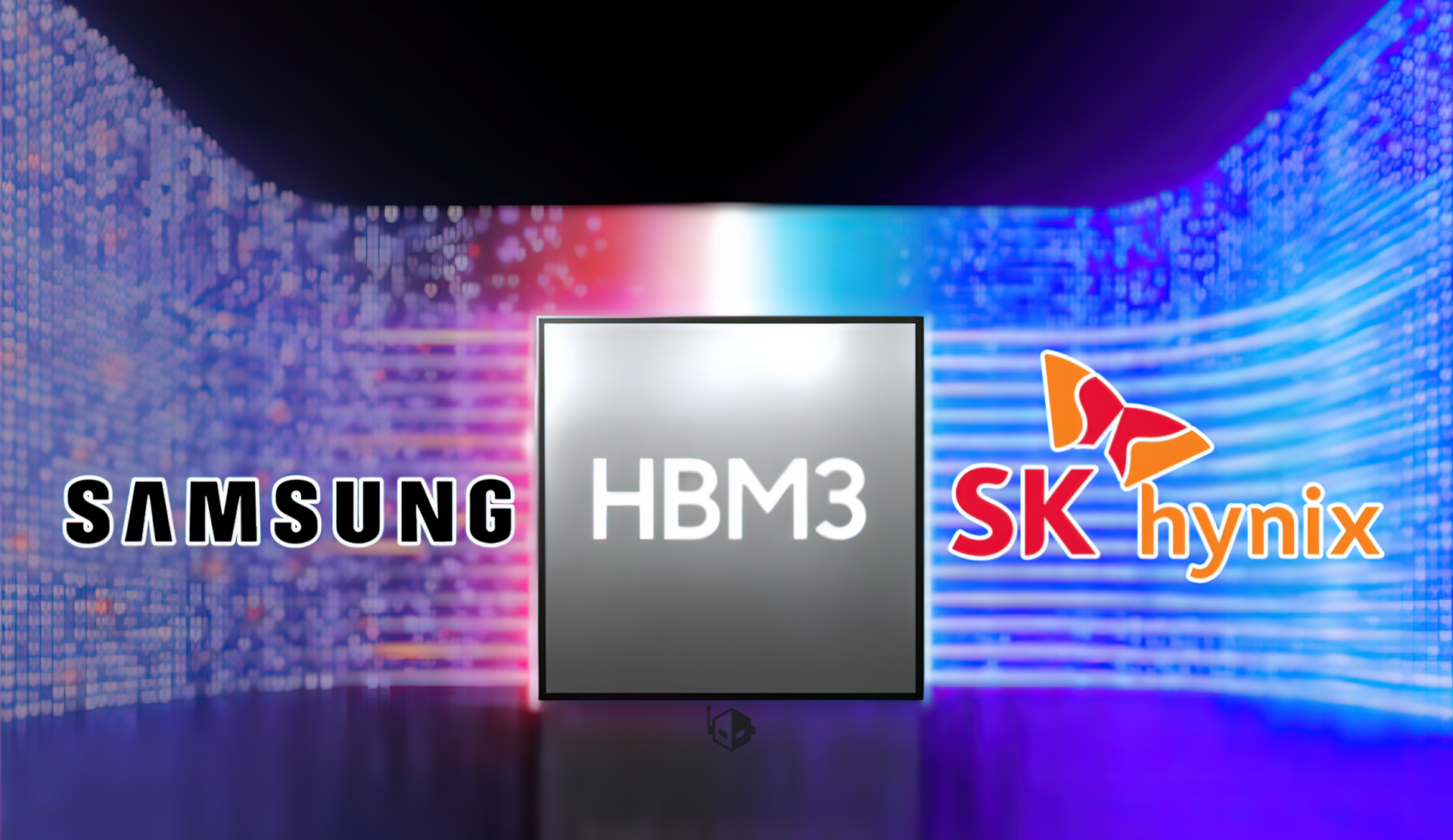
Is SK hynix the only one developing this technology? No, the HBM market is highly competitive. Companies like Samsung and Micron are also investing heavily in next-generation HBM technologies and advanced packaging techniques to meet the surging demand from AI and HPC sectors.