AI is the new silicon.
This isn’t just a catchy tagline; it’s the fundamental truth unfolding within TSMC, the undisputed titan of chip manufacturing. We’ve seen AI revolutionize what goes onto the chip – accelerating designs, enabling complex algorithms, and powering everything from your phone to self-driving cars. But now, AI is becoming the warp drive for the fabs themselves. Dr. Cliff Hou’s recent pronouncements on TSMC’s N2 process technology aren’t just about faster transistors; they’re a seismic announcement that AI is now deeply embedded in the very creation of these nanoscale marvels.
AI Remakes the Foundry Floor
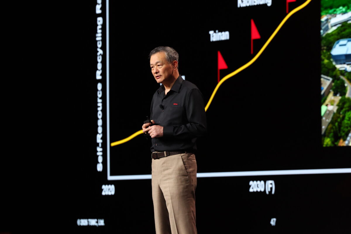
Forget the image of meticulous, but slow, human processes dictating every step. TSMC is explicitly stating that AI is the secret sauce behind their astonishing N2 ramp. We’re talking about AI-driven systems optimizing scheduling, fine-tuning equipment efficiency, and slashing production cycle times. Generative AI is even being deployed to meticulously tweak process parameters, pushing the boundaries of what’s possible. This isn’t just about squeezing a bit more out of existing machinery; it’s a fundamental transformation, allowing TSMC to extract far greater productivity from their current capacity while new, behemoth fabs are being constructed. It’s like discovering a cheat code for physics, enabling them to build more, faster, and better than anyone imagined.
Consider this: TSMC is ramping up five phases of 2nm (N2) fabs within a single year. That’s an absolutely wild pace. And the projected first-year output for 2nm is a staggering 45% higher than that of the previous 3nm generation. This isn’t just incremental progress; it’s a quantum leap, and the article points to AI and digital transformation as the key enablers. It’s a profound statement about the future of manufacturing, where intelligence isn’t just a product of the chips, but an active participant in their birth.
This is more than just a tech update; it’s a window into a fundamental platform shift. AI isn’t just an application anymore; it’s becoming the foundational layer upon which entire industries are being rebuilt. We’re witnessing the birth of AI-native manufacturing, where sophisticated algorithms are as critical as photolithography equipment.
Demand for the AI Engine
The relentless hunger for AI and High-Performance Computing (HPC) applications is, unsurprisingly, a massive driver of this frenzy. The numbers are simply astronomical: from 2022 to 2026, the number of wafers shipped for AI accelerators is expected to increase elevenfold. Elevenfold! And it’s not just about more chips; it’s about bigger chips. Large-die chips (over 500 mm²) are also experiencing explosive growth, with shipments increasing sixfold. This is where TSMC’s decades of experience across multiple generations truly shine. They’ve honed their craft, ensuring consistent improvements in yield and defect density, even for these gargantuan, complex designs that would have been science fiction a decade ago.
TSMC’s accumulated experience across multiple generations has enabled consistent improvements in yield and defect density, even for these complex designs.
That quote, plucked directly from the material, underlines the silent, unglamorous but utterly essential work that happens behind the scenes. It’s the years of painstaking refinement that allow for the audacious leaps we’re seeing now.
Beyond the Bleeding Edge: Mature Nodes and Packaging Prowess
While N2 and AI get the headlines, TSMC isn’t abandoning its bread-and-butter. They continue to invest heavily in mature nodes, ensuring a steady supply of specialty processes like radio frequency, high-voltage, analog, embedded memory, and image sensors. This strategic diversification is smart business, keeping them dominant across the entire semiconductor spectrum.
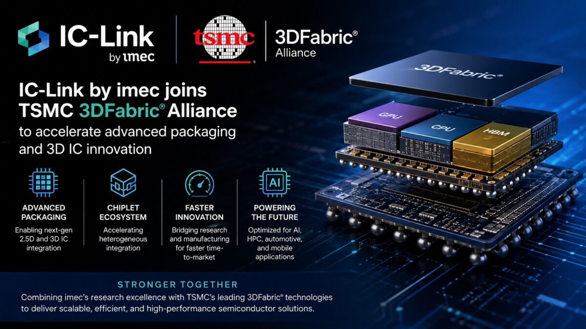
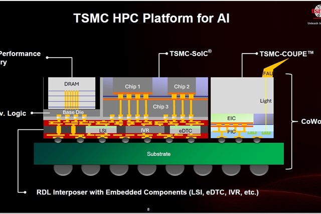
And then there’s advanced packaging – the complex art of stacking and connecting multiple chiplets. Technologies like CoWoS and SoIC are becoming absolutely critical for enabling the chiplet-based architectures that are increasingly favored for their flexibility and performance. The fact that TSMC has dramatically reduced the transition time from development to high-volume manufacturing for these complex packaging solutions — a 30% cut for CoWoS and an astonishing 75% for SoIC — is another proof to their relentless pursuit of speed-to-market for their customers. They’re not just making chips; they’re enabling entire product ecosystems to come alive faster than ever before.
Why Does This Matter for Developers?
For developers, this is more than just news about silicon. It’s about access. The foundation of TSMC’s success, particularly through Dr. Hou’s efforts in building the Open Innovation Platform (OIP), has been about democratizing chip design. By lowering barriers to entry and providing strong design enablement infrastructure (think design kits and reference flows), TSMC has made complex IC design accessible to a much wider audience. This continued push for advanced nodes and sophisticated packaging, coupled with AI-driven manufacturing efficiency, will only serve to further accelerate the innovation cycle. More powerful, more efficient, and potentially more accessible custom silicon will become the norm. We’re talking about a future where specialized AI accelerators, custom logic, and novel memory configurations can be brought to market with unprecedented speed and at potentially more digestible costs for a broader range of companies.
This is the exciting part of this platform shift: it’s not just for the hyperscalers anymore. As the underlying manufacturing becomes more efficient and more intelligent, the benefits trickle down, empowering smaller teams and new ventures to dream bigger. The potential for bespoke silicon tailored for specific AI tasks, for instance, becomes far more realistic.
🧬 Related Insights
- Read more: Arm Breaks Its Licensing Habit With the AGI Server CPU
- Read more: How Semiconductor Fabrication Works: From Silicon Wafer to Finished Chip
Frequently Asked Questions
What is TSMC’s N2 process technology? TSMC’s N2 is their most advanced semiconductor manufacturing node, utilizing 2-nanometer (nm) process technology. It represents a significant leap in transistor density, performance, and power efficiency compared to previous generations like N3 (3nm).
How is AI being used in TSMC’s manufacturing? TSMC is employing AI for various aspects of chip production, including optimizing production schedules, enhancing equipment efficiency, fine-tuning process parameters, and minimizing manufacturing downtime. This digital transformation is accelerating yield learning and production ramp-up.
Will TSMC’s N2 technology be available to everyone? TSMC’s business model is to provide manufacturing services to other companies (foundry model). While N2 is their leading-edge technology, its availability and cost will depend on the specific agreements and chip designs of their customers, which include major tech companies and increasingly, specialized AI firms.