Look, nobody in this business likes waiting. Especially not for simulations. For the longest time, thermal analysis for these monstrous 2.5D High Bandwidth Memory (HBM) packages has been a black hole of time and resources. We’re talking about chips that are literally stacks of memory piled on top of ASICs, all crammed together on an interposer, cooking themselves into oblivion. Everyone expected a breakthrough, something that would cut down the agonizing months spent tweaking designs, something to finally keep pace with how fast these things are being built. And here we are, with Vinci, promising just that: deterministic, solver-accurate thermal and warpage analysis at manufacturing resolution. Sounds fancy, right? Let’s see if it’s more than just PR fluff.
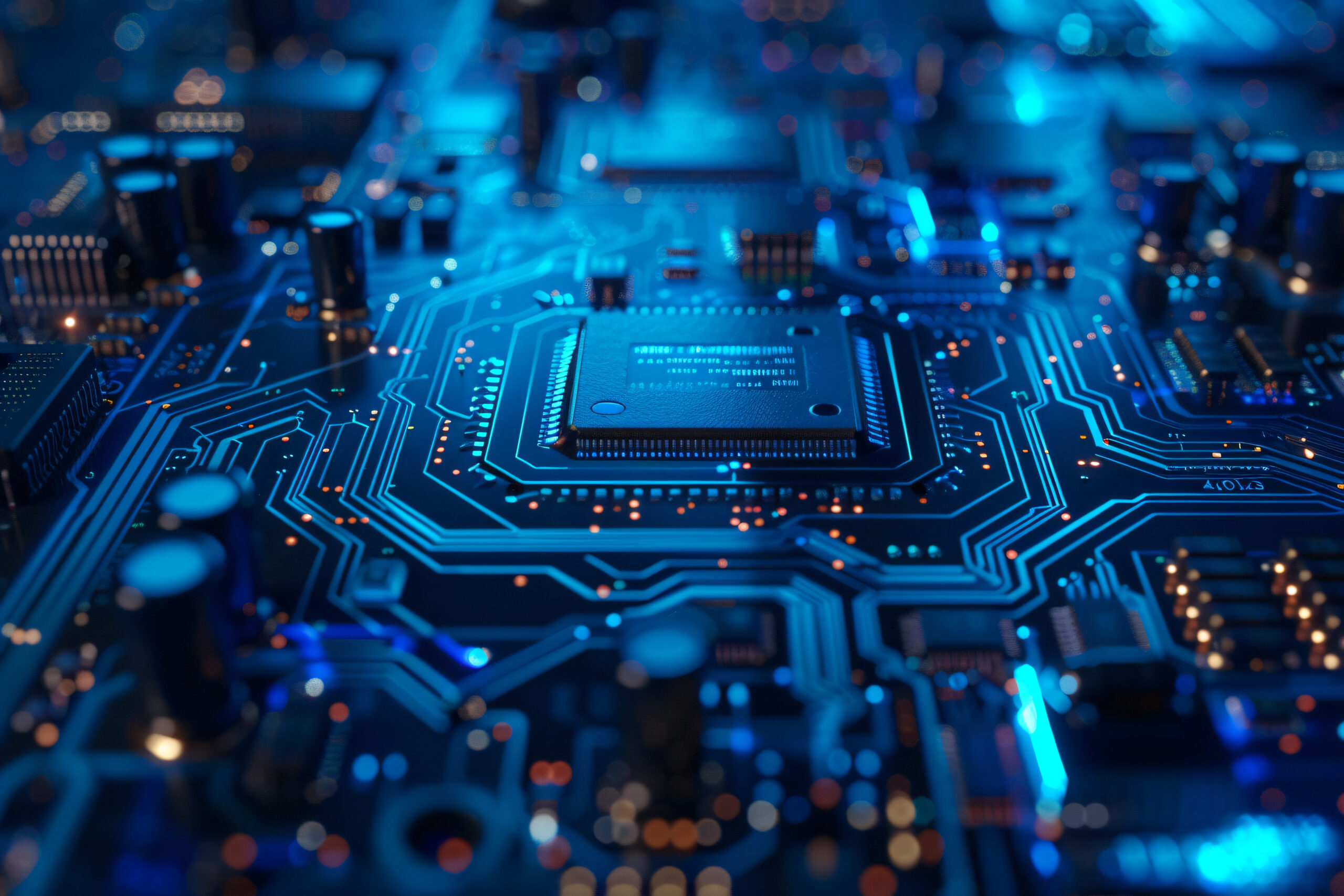
Thermal management. That’s the buzzword de jour, isn’t it? It’s the bogeyman under the bed for anyone trying to push the boundaries of high-performance computing and AI accelerators. These modern packages are absolute beasts, jamming together high-power ASICs with multiple HBM stacks. The problem is, they’re all so tightly coupled thermally and mechanically that you get this nasty feedback loop. You’ve got heat bleeding from one chip to another, cranking up HBM temperatures. Then, you have the materials – epoxy molding compounds, silicon interposers, organic substrates – all expanding and contracting at different rates due to temperature changes. This differential expansion, this CTE mismatch, it warps the whole darn thing, threatening the microscopic solder joints that hold it all together. Reliability? Forget about it.
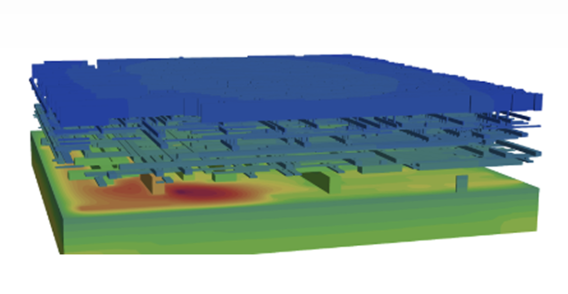
And the HBM stacks themselves are getting insane. Remember when four HBM dies stacked vertically was a lot? Now we’re seeing up to 16. Sixteen! All crammed into these tight columns next to the main ASIC. When you’re talking about systems packing four or more of these monsters, you’re staring down an aggregate thermal design power that can easily blow past 1 kilowatt. A kilowatt! That’s like running a high-end toaster oven inside your server rack. At this power density, you can’t afford to generalize. You need to see the tiny hotspots forming at the tier level, track how heat crawls through the Through-Silicon Vias (TSVs), and account for the weird, directional resistance across the backend-of-line layers and those fiddly micro-bump arrays. To really capture all this, you need simulations that look at the geometry at the actual manufacturing level. No shortcuts. No simplified models.
So, what’s the hold-up? Why aren’t we already there? Conventional Finite Element Analysis (FEA), the workhorse for these kinds of problems, just can’t cut it. It’s fundamentally too slow and too coarse. Trying to cram the insane detail of a real manufacturing process into an FEA model is like trying to stuff an elephant into a sardine can – it just breaks. It either takes eons to run, or the results are so generalized they’re practically useless for catching the real failure points.
This is where Vinci steps in, or at least claims to. They’re touting this system as a way to perform deterministic, solver-accurate physics computations directly on manufacturing-resolution geometry. They’ve run it on a representative 2.5D package, and the results, they say, are a game-changer. They claim it bypasses the usual simplifications that plague traditional methods, allowing for unprecedented accuracy at speeds that actually make sense for modern design cycles. Who’s actually making money here? Well, the companies building these advanced packages are hemorrhaging money on development time and potential failures. If Vinci can deliver even a fraction of its promises, the savings could be massive.
Is Vinci Actually Faster? The Billion-Dollar Question
The core promise of Vinci is speed. Traditional FEA solvers, when faced with the sheer complexity of modern 2.5D HBM packages – with their complex multi-layer stackups, BEOL metal layers, micro-bump arrays, and TSVs – buckle under the weight of the computational load. Simplifications are made, and often, those simplifications mean missing critical thermal hotspots or warpage issues. Vinci claims to sidestep this by working directly with the manufacturing-level geometry. This means no aggressive meshing or geometry simplification, which are often the bottlenecks in FEA. If they’ve managed to optimize their solver to handle this data density efficiently, we could be looking at a significant reduction in simulation times, moving from weeks or months down to days or even hours.
“Capturing these effects requires simulation at manufacturing resolution.”
This quote, right from their own material, is the crux of the problem. They’re acknowledging the need for detail, a detail that current tools struggle with. The question isn’t if manufacturing resolution is needed, but how you get there without collapsing your entire compute infrastructure and design timeline. Vinci’s approach, by directly computing on this geometry, is certainly an interesting angle. It’s a bit like ditching the blueprint and working directly off the assembly line schematics, but for physics.
So, Who’s Benefiting Here?
Let’s be brutally honest. Silicon Valley runs on hype, and this sounds like a good dose of it. But beneath the jargon, there’s a real problem. The companies designing these advanced packages – think AMD, Intel, NVIDIA, and their packaging partners – are spending fortunes. Every design iteration, every bug found in simulation that could have been caught earlier, adds to the bottom line. If Vinci can truly deliver accurate thermal and warpage predictions quickly, the potential return on investment is enormous. We’re talking about reducing costly respins, improving product performance by optimizing cooling, and ensuring long-term reliability, which is always a PR nightmare waiting to happen.
This isn’t just about making chips faster; it’s about making them survive. These advanced packages are pushing the limits of what physics allows. When you pack that much power into such a small space, and then expect it to operate reliably for years in a server farm or a high-end workstation, you need absolute confidence in your thermal and mechanical design. Vinci’s claim to offer this confidence at manufacturing resolution is, if true, a massive win for the engineers on the ground and the bean counters in the boardroom.
🧬 Related Insights
- Read more: Micron’s Virginia Fab Sparks US DRAM Race [Advanced Memory]
- Read more: Prebuilt Gaming PC Slashed $500: RTX 5060 Ti, Ryzen 7800X3D for $1599
Frequently Asked Questions
What does Vinci’s ‘deterministic, solver-accurate’ analysis actually mean?
It means they claim their simulation results are precise and predictable, directly reflecting the physics of the manufacturing-level geometry without the guesswork or approximations often found in traditional, generalized simulation methods.
Will this make my AI chips run cooler?
Potentially. By providing more accurate and faster analysis, engineers can identify and fix thermal issues earlier in the design process, leading to better-cooled and more reliable chips.
Is this a new type of chip packaging technology?
No, Vinci is a software system for simulating and analyzing existing 2.5D HBM package designs, not a new hardware packaging method itself.