Look, nobody likes surprises. Especially not engineers who’ve poured years into designing a complex chip only to find out it melts under load. That’s the dirty little secret about fancy new multi-die designs: they’re not just complicated; they’re a chaotic soup of electrical, thermal, electromagnetic, and even mechanical headaches all mashed together. And guess what? You can’t just slap a fan on it and call it a day anymore.
This isn’t some abstract academic exercise. This is about whether the phone in your pocket will spontaneously combust or if that cutting-edge AI accelerator will actually perform as advertised. For too long, the industry treated these ‘multiphysics’ problems—the messy interactions between different physical forces—as an afterthought. Like a bad sequel, they hoped it would just work out. It rarely did.
Why the Last-Minute Rush is Dead
The old way? Design, design, design, then cross your fingers and run a bunch of tests right before manufacturing. If you found a problem, it was a disaster. Think expensive respins, missed deadlines, and a whole lot of managerial hand-wringing. With designs now stacking multiple chips (dies) on top of each other, these interactions aren’t just lurking; they’re in your face. Electrical interference can mess with thermal sensors. Heat can warp delicate structures. It’s a domino effect of potential failure.
This new approach, forcing multiphysics analysis earlier in the design flow, isn’t about innovation. It’s about survival. It’s admitting that the old model was fundamentally flawed for the complexity we’re dealing with now.
So, What’s the Big Idea?
The core pitch here is simple: unify everything. Stop treating electrical simulation, thermal simulation, and the like as separate silos. They need to talk to each other, constantly, from the initial sketch of the chip right through to the final sign-off before manufacturing. This means a continuous validation process. You build a piece, you test its physical interactions, you tweak, you repeat. It’s like building a skyscraper with a constantly updated structural integrity report for every floor, not just waiting for the final inspection.
The promise is a smoother ride. Fewer nasty surprises. And, hopefully, chips that actually do what they’re supposed to without setting off smoke alarms.
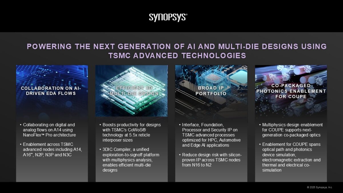
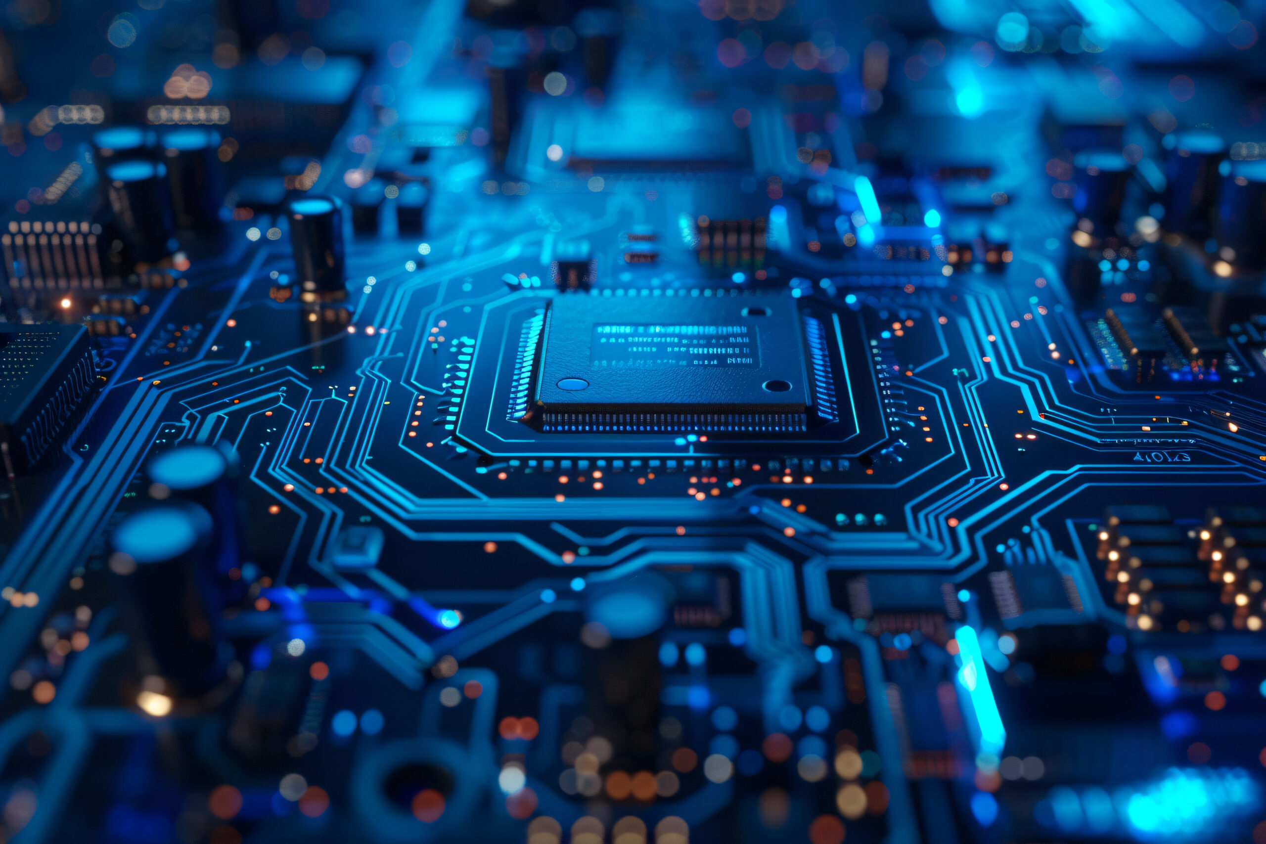
Multiphysics issues are no longer a late-stage problem. Multi-die designs introduce tightly coupled electrical, thermal, electromagnetic, and electromechanical challenges that impact performance and reliability.
This isn’t just a technical shift; it’s a cultural one. It requires a different mindset and, crucially, the right tools that can handle this integrated approach. Companies that cling to the old ways are going to be left in the silicon dust, dealing with costly recalls and underperforming products. The ones that embrace this early, unified analysis? They’re the ones building the future, one less-flammable chip at a time.
What This Means for Your Gadgets
For the average Joe or Jane, this means better. More reliable devices. Faster phones that don’t overheat after five minutes of gaming. AI accelerators that can actually handle the massive datasets they’re fed. It’s the difference between a device that feels premium and one that feels… cheap and likely to fail prematurely. It’s about ensuring the silicon you’re paying for is actually fit for purpose, not a barely-contained inferno.
This shift is a tacit admission by the industry that the “move fast and break things” mantra, while catchy, has real-world consequences when applied to hardware. And those consequences are often thermal.
The PR Spin vs. Reality
Of course, the vendors will spin this as a marvel of engineering. They’ll talk about ‘synergy’ and ‘advanced workflows.’ Don’t be fooled. This is a necessity born out of a problem they helped create with increasingly complex, stacked architectures. The real story is that their old methods were insufficient. This is less a revolutionary leap and more a frantic scramble to catch up with the engineering reality of bleeding-edge chip design. It’s good they’re finally addressing it, but let’s not pretend it’s a sudden burst of altruism; it’s a practical, albeit overdue, adjustment.
**
🧬 Related Insights
- Read more: MacBook Pro + RTX 5090: Over 100 FPS Cyberpunk via eGPU [Analysis]
- Read more: RTX 5090 Humiliates $30K AI GPUs in Password-Cracking Showdown
Frequently Asked Questions**
Will this make my computer overheat less?
Potentially. By catching thermal issues early in the design process, manufacturers can build more efficient cooling solutions and optimize chip performance to prevent overheating. It’s about building cooler, not just faster, chips.
Is this only for super-high-end chips?
While the impact is most pronounced in complex multi-die designs for AI, high-performance computing, and advanced mobile devices, the principles of early multiphysics analysis can benefit a wide range of silicon development, leading to more reliable products overall.
Does this mean longer design times?
It can mean an initial adjustment in the design cycle as teams adopt new tools and methodologies. However, the goal is to reduce costly design respins and late-stage problem-solving, ultimately leading to faster time-to-market for reliable products.