The stench of burning silicon and desperation – that’s what this whole “reshoring” semiconductor manufacturing smells like. Another company, another shiny new facility, another round of breathless pronouncements about a new era. This time it’s Custom Interconnect Ltd. (CIL), a UK outfit, unfurling its new 64,000-square-foot facility they’re calling BP2. Apparently, it’s the largest semiconductor packaging operation in the UK. Which, let’s be honest, isn’t exactly setting a high bar. But hey, in the current climate, where every critical component is a potential geopolitical weapon, maybe that’s exactly the point.
For years, the mantra was simple: China, Taiwan, South Korea. Cheaper labor, massive scale, all the infrastructure already in place. Why would anyone with a shred of fiscal sanity build chips elsewhere? The answer, as it turns out, is ‘because the world is on fire.’ Rising tensions, you know the drill. Suddenly, those efficient global supply chains look less like a marvel of modern logistics and more like a very long, very fragile string just waiting to snap. And when it snaps, guess who’s left holding the very expensive, very broken pieces?
Governments are scrambling, throwing billions at the problem. The US has its CHIPS Act, Europe has its own hefty €43 billion play. It’s a global land grab for semiconductor sovereignty, or at least the illusion of it. But CIL, bless their ambitious hearts, aren’t waiting for Uncle Sam or the EU to throw them a handout. They’ve decided to go it alone, plunking down their own cash for BP2. Nearly four decades in the electronics game, and now they’re venturing into the deep end of semiconductor assembly and packaging.
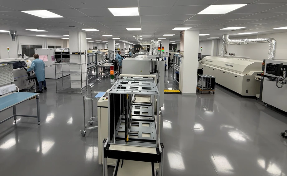
The Shiny New BP2: What’s Actually Inside?
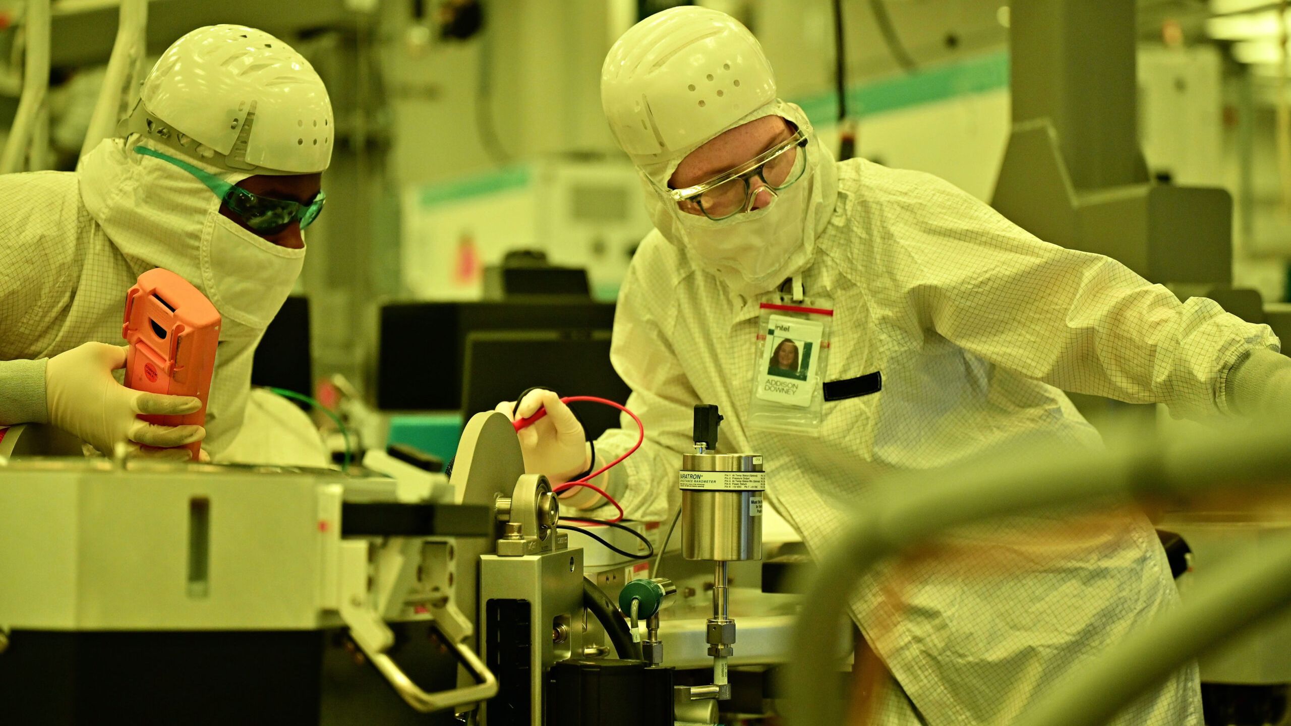
This BP2 place isn’t just another assembly line. They’re touting wafer-level chip-scale packaging (WLCSP) and flip-chip solder bumping for 2.5D integration. And they’re poking around 3D stuff with solder joints smaller than a dust mite. It’s a 15,000-square-foot ISO 7 cleanroom, which sounds sterile enough to perform surgery on a microchip. Special lighting for wafer dicing – because apparently, you can’t just chop up silicon in the dark. The big selling point? The “smoothly workflow” linking PCB assembly and semiconductor packaging. They can either take a bare chip, slap it onto a board, wire it up with gold or aluminum, and seal it. Or, they can take a wafer, chop it up, package the individual dice, and then stick those into boards. It’s a two-way street, apparently. They can even make custom QFN packages.
They’re claiming support for wafers up to 300mm, handling silicon, gallium arsenide, gallium nitride – the whole gang. This isn’t just stuffing components onto a printed circuit board anymore; CIL is wading into actual semiconductor manufacturing territory. Who’s actually making money here? Well, if you’re a UK company that suddenly can’t get your chips from Asia, and CIL can deliver something, you’re probably willing to pay a premium. CIL’s bet is that the pain of disruption outweighs the cost of domestic production.
This isn’t just about a new facility; it’s a bet against globalization’s ever-present tail risk. For years, the cost savings were undeniable. Now, the cost of insecurity is rapidly catching up. CIL’s move is less about innovation and more about old-fashioned risk mitigation. They’re building a moat. A very expensive, very clean moat.
The Pragmatic Shift: Beyond the Hype
Let’s cut through the jargon. What CIL is doing is packaging, not fabricating raw silicon from sand. Fabrication is the really big, dirty, astronomically expensive game. Think TSMC and Intel. Packaging is the step after the wafer has been made, where the individual chips are prepared for use. It’s still critical, and yes, it’s a bottleneck CIL is now trying to address domestically. Their ability to handle various materials and integration methods is certainly noteworthy. The claim of having the only UK system for WLCSP and flip-chip is the kind of specific detail that makes you pause. It suggests a genuine capability, not just a broad-stroke investment.
The question that always hangs in the air with these kinds of announcements is: can they scale? Can they do it consistently? And most importantly, can they do it at a price that doesn’t make customers run screaming back to the offshoring model the moment supply chains stabilize? The “smoothly workflow” sounds nice, but the devil, as always, is in the execution. One faulty wire bond, one contaminated cleanroom, and that carefully constructed domino chain falls apart. The sheer volume of components they’re claiming to process per day – a million SMT placements, 1.5 million wire bonds per week – is staggering, if accurate. That’s the kind of throughput that starts to look like a serious contender, assuming quality holds.
“The BP2 site represents the largest semiconductor packaging operation in the UK, combining high-volume PCBA production with a 15,000 sq ft ISO 7 cleanroom dedicated to semiconductor assembly.”
This isn’t a revolution in chipmaking, but it’s a pragmatic response to a very real, very unglamorous problem. The days of ‘set it and forget it’ global sourcing are over, at least for now. Companies are going to pay a premium for reliability. CIL is positioning itself to be that reliable, domestic option. The ultimate winner here, beyond CIL itself, might just be the notion that resilience, not just cost, is king. It’s an expensive lesson for everyone involved, but one we’re clearly being taught in real-time.
🧬 Related Insights
- Read more: Nvidia’s $20 Billion Groq Heist: GPU Kingpin Bows to Inference Rebels
- Read more: NVIDIA AI Costs Outpace Human Pay
Frequently Asked Questions
What does Custom Interconnect Ltd. (CIL) actually do? CIL is an electronics manufacturing services company specializing in PCB assembly and, with their new BP2 facility, advanced semiconductor packaging and assembly. They work with components from initial design through to finished product.
Will this new UK facility mean cheaper chips? Unlikely in the short term. The primary driver for this investment is supply chain resilience and domestic capability, not cost reduction. While increased competition can eventually drive down prices, the initial focus is on providing a reliable, UK-based alternative to offshore manufacturing, which often comes at a premium.
Is this a full chip fabrication plant? No. CIL’s BP2 facility focuses on semiconductor packaging and assembly – the process of preparing manufactured silicon wafers and chips for integration into electronic devices. Chip fabrication, which involves creating the actual silicon wafers, is a much more complex and capital-intensive process typically done by large foundries like TSMC or Intel.