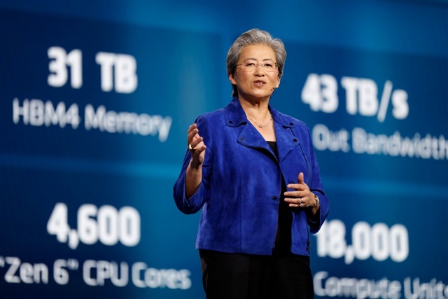
The air in Suzhou last Monday, May 20th, carried the distinct hum of ambition and consequence. AMD CEO Lisa Su stood center stage, not at a product launch, but at the ribbon-cutting ceremony for the second-phase expansion of Suzhou TF-AMD Semiconductor Co. This isn’t just another factory opening; it’s a stark indicator of where AMD sees its future, particularly when it comes to the complex, final stages of chip production: advanced packaging.
It’s easy to dismiss this as routine capacity building. But look at the numbers: the expansion of TF-AMD, AMD’s joint venture with Nantong Fujitsu Microelectronics (a subsidiary of China Electronics Corporation), signifies more than just a bigger footprint. It represents a deepening strategic alliance in a sector that is increasingly defined by geopolitical fault lines and supply chain vulnerabilities. Advanced packaging, the art of putting multiple chips or components together in a single package, is no longer an afterthought. It’s a critical differentiator, influencing performance, power efficiency, and cost.
Why Suzhou Matters for AMD’s Packaging Strategy
AMD’s commitment here is substantial. The expansion aims to bolster its capacity for advanced packaging technologies like chiplets, a cornerstone of its Zen architecture and its strategy to compete more effectively in high-performance computing. For years, China has been a powerhouse in assembly, testing, and packaging (ATP), but the move towards advanced techniques like 2.5D and 3D stacking requires significant investment and technological prowess. AMD, by pouring resources into TF-AMD, is effectively co-investing in China’s evolution from a mass assembler to a more sophisticated player in the semiconductor value chain.
This isn’t just about fulfilling current demand; it’s about de-risking. While the West pushes for domestic chip manufacturing and R&D, the reality of the global semiconductor ecosystem is that it’s deeply interconnected. Trying to disentangle it entirely is a fool’s errand. AMD’s strategy here, like many others in the industry, is a pragmatic acknowledgment of this reality. They’re diversifying their risks by strengthening their partnerships in key existing hubs, rather than attempting a full, immediate, and likely prohibitively expensive relocation of all advanced packaging operations.
Geopolitical Tightrope Walk
Of course, no discussion of China and advanced technology is complete without a nod to the escalating geopolitical tensions. The U.S. has been increasingly vocal about restricting China’s access to advanced semiconductor technology, ostensibly for national security reasons. However, the sophisticated nature of advanced packaging presents a unique challenge. It often involves proprietary processes and equipment that are not easily replicated or sanctioned without significant disruption to the entire global supply chain. AMD’s expansion, therefore, can be seen as a calculated move to secure critical packaging capacity while navigating these thorny international relations. It’s a delicate balancing act.
“AMD’s investment in Suzhou underscores the critical role of advanced packaging in our product strategy and the long-standing importance of our partnership with our customers and stakeholders in China.”
That quote, from a company representative, is diplomatic but telling. It highlights the “long-standing importance” of their China operations, framing the expansion as a continuation of established relationships rather than a purely new initiative. It’s a smart PR move, but the underlying market dynamics are far more complex.
The ‘Chiplet’ Revolution and China’s Role
The industry is increasingly embracing a chiplet-based design philosophy, where smaller, specialized processing units are interconnected within a single package. This approach offers greater flexibility, improved yields, and cost efficiencies compared to monolithic chip designs. AMD has been a pioneer in this space with its Ryzen and EPYC processors. For these chiplets to work their magic, they need to be smoothly integrated through advanced packaging. China, with its established infrastructure and growing technical expertise, is a natural, if politically charged, partner in this evolution. Denying access to this capability would hamstring not only Chinese manufacturers but also global players like AMD who rely on that capacity.
So, what does this expansion ultimately mean? For AMD, it’s about securing essential manufacturing capabilities and maintaining a competitive edge in a market that demands both cutting-edge performance and cost-effectiveness. For the global semiconductor industry, it’s a clear signal that advanced packaging remains a concentrated area of expertise, with China playing an indispensable, albeit increasingly scrutinized, role. Expect more companies to follow similar strategies: doubling down on existing, proven infrastructure while cautiously exploring diversification elsewhere. It’s not a retreat from the West, but a pragmatic embrace of the East’s current capabilities.
What’s Next for Chip Packaging?
This expansion isn’t the end of the story. It’s a chapter in a much larger narrative about supply chain resilience, technological innovation, and the enduring importance of specialized manufacturing hubs. As the demand for more powerful and efficient processors continues to soar, driven by AI, high-performance computing, and advanced graphics, the importance of advanced packaging will only grow. AMD’s Suzhou play is a high-stakes bet on this future, a bet that acknowledges the complex, interwoven reality of global chip production.
🧬 Related Insights
- Read more: Kubb Mini PCs: Color in a Silent World
- Read more: 007 First Light: Series S 30 FPS Cut Is About RAM, Not Just Dev Laziness
Frequently Asked Questions
What is advanced packaging in semiconductors? Advanced packaging refers to the methods used to assemble and connect semiconductor chips and components into a final product package. It includes techniques like chiplets, 2.5D and 3D stacking, which improve performance, power efficiency, and reduce size, moving beyond traditional single-chip integration.
Will this expansion impact AMD’s US manufacturing? AMD’s expansion in Suzhou is focused on advanced packaging, a specific segment of the semiconductor manufacturing process. While AMD, like other semiconductor companies, is also investing in domestic manufacturing and R&D in the US and other regions, this Suzhou initiative aims to bolster their global packaging capacity and doesn’t directly replace existing or planned US-based fabrication or advanced packaging facilities.
Is AMD reducing its reliance on China with this move? No, this expansion represents an increase in AMD’s investment and focus on advanced packaging in China. It signifies a strategic deepening of their partnership in this region, rather than a diversification away from it. It’s a pragmatic approach to leveraging existing, advanced capabilities to meet global demand.