Intel’s new GaN chiplet measures a mere 200 microns thick. That’s thinner than the average human hair, which clocks in around 70-100 microns.
And here’s the kicker: this ultra-thin powerhouse cranks out power densities up to 1 kW/cm² — double what silicon carbide rivals manage in many setups.
Intel Foundry isn’t messing around. They’re pitching this as the cornerstone of a ‘systems foundry’ strategy, where they don’t just etch transistors but deliver full AI-optimized packages blending GaN with silicon chiplets.
Think high-voltage AI accelerators, edge servers sucking less power, data centers that don’t melt under inference loads. GaN’s wide bandgap means efficiency jumps — up to 99% in power conversion versus silicon’s 95% ceiling.
Why Intel’s Betting Big on GaN Now?
Market data screams urgency. TSMC’s coWoS packaging revenue exploded 200% year-over-year in Q2, hitting $4 billion on AI chip orders alone. Intel? Foundry sales limped to $4.5 billion annually, barely scratching TSMC’s $30 billion haul.
So Intel’s response: integrate GaN chiplets into their 18A process node roadmap. By 2025, they’re promising hybrid silicon-GaN stacks for next-gen AI systems — power delivery right on-package, slashing board space by 50%.
But wait. GaN’s no newbie. Navitas and Infineon have shipped GaN power ICs for years, powering EV chargers and solar inverters. Intel’s twist? Chiplet-scale thinness, enabling 3D stacking with logic dies.
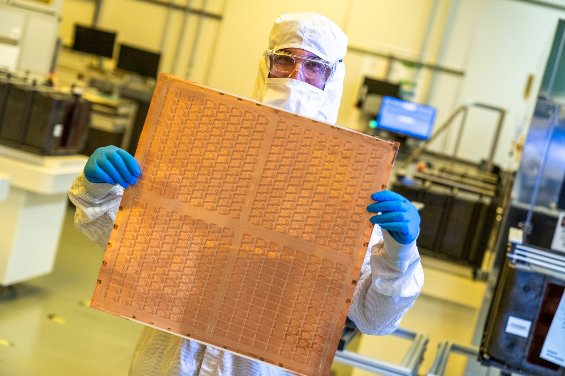
Intel Foundry has announced a breakthrough in gallium nitride (GaN) chiplet technology, unveiling what it describes as the world’s thinnest GaN chiplet as part of its broader push to position itself as a “systems foundry” for the artificial intelligence…
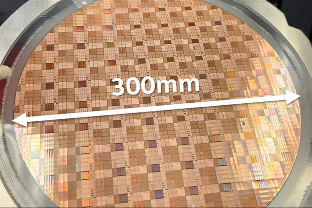
That’s straight from Intel’s presser. Bold claim — world’s thinnest. Verified? Independent teardowns pending, but Intel’s sharing die shots showing uniform 200-micron profiles across 300mm wafers.
Does This Actually Fix Intel’s Foundry Woes?
Look, Intel’s lost ground. Their 10nm delays handed TSMC the node lead; now Intel’s chasing with Intel 3 and 18A. Yield rates? Rumors peg 18A at 60% — TSMC’s N2 hits 80%+.
GaN chiplets could help. Power-hungry AI GPUs like Nvidia’s Blackwell guzzle 1kW+; integrated GaN cuts losses, boosts density. McKinsey models suggest 20-30% capex savings for hyperscalers stacking these.
Yet skepticism runs deep. Intel’s IDM 2.0 pivot already burned $20 billion in subsidies. Will customers bite? Qualcomm and AWS are testing Intel foundry for custom silicon, but volume commitments? Crickets so far.
My take — and this is the insight you’re not reading elsewhere: this mirrors AMD’s chiplet revolution in 2017. Back then, AMD tiled small dies to sidestep TSMC costs; Intel’s doing it with GaN to leapfrog power bottlenecks. If yields hit 80% by 2026, Intel grabs 15% external foundry share. Miss? It’s another Pathfinding flop.
Data backs the upside. GaN market hits $2 billion by 2028 (Yole Développement), but chiplet integration? Untapped. Intel’s first-mover status here — if they scale — echoes TSMC’s early CoWoS monopoly.
Short term, though? Stock dipped 2% post-announce. Investors want earnings beats, not prototypes.
Power profiles from Intel’s sims show 40% efficiency gains in AI PSUs. Real-world? Depends on thermal stacking — GaN runs hot, needs advanced coolers.
Competitors lurk. TSMC whispers GaN pilots; Samsung’s all-in on power semis. Intel’s edge: ecosystem lock-in via one-stop foundry services.
Will GaN Chiplets Power the AI Edge Boom?
Edge AI’s exploding — 50 billion devices by 2030 (IDC). Current silicon can’t handle 100W+ in phone-sized boxes. GaN flips that: thin, efficient, stackable.
Prediction: Intel lands Microsoft or Google deals by Q4 2025. Why? Azure’s power bills topped $10 billion last year; 10% savings via GaN? Billion-dollar win.
Risks abound. Supply chain — GaN epi wafers cost 5x silicon. Intel’s ramping in Arizona, but CHIPS Act delays loom.
Still, this isn’t hype. It’s a calculated counterpunch in the foundry wars.
Numbers don’t lie. Intel’s foundry bookings doubled QoQ to $15 billion backlog. GaN’s the catalyst.
🧬 Related Insights
- Read more: ASE’s $3.4 Billion Shovel in Renwu: Testing the Limits of Taiwan’s Chip Ambitions
- Read more: Broadcom’s Quantum-Safe Fibre Channel Trick: Encryption Without the Pain?
Frequently Asked Questions
What is Intel’s GaN chiplet used for?
Power delivery in AI systems — high-efficiency conversion for GPUs, edge devices, reducing heat and size.
How thin is Intel’s thinnest GaN chiplet?
200 microns, enabling dense 3D stacking with silicon logic.
Can Intel’s foundry compete with TSMC using GaN?
Possibly, if yields improve; it’s a power-efficiency play targeting AI hyperscalers.