Shovels bite into Taiwanese soil. April 10, 2026, Renwu Industrial Park — ASE Test, the testing arm of the world’s top OSAT, kicks off what they’re calling a game plan for the future of chip validation.
It’s not just dirt-moving. This $3.4 billion push — ASE’s biggest yet in advanced processes — teams them up with WinWay and Horng Terng Automation (HTA), aiming to crank out testing for bleeding-edge nodes, think 2nm, chiplets, maybe even co-packaged optics down the line.
Global OSAT leader ASE continued its expansion into advanced processes as its subsidiary ASE Test held a groundbreaking ceremony on April 10, 2026, at the Renwu Industrial Park. ASE collaborated with WinWay and Horng Terng Automation (HTA) to jointly…
Zoom out. ASE isn’t building another assembly line. They’re chasing the ‘how’ of testing complexity — why chips now demand insane parallelism in validation, electrical probing at sub-atomic scales, thermal cycling that mimics hellish data center runs. It’s the unglamorous backend where yields live or die.
Here’s the thing. Taiwan’s OSAT kings like ASE have feasted on packaging booms, but testing? That’s the new bottleneck as AI hyperscalers shove HBM4 and beyond down everyone’s throat.
Why Renwu? Taiwan’s Secret Weapon Against Offshore Drift
Pick a spot like Renwu — Kaohsiung outskirts, primed with power grids, skilled labor pools from nearby fabs. But dig deeper: it’s a stone’s throw from ASE’s existing Hsinchu ops, slashing logistics bleed. No shipping delicate testers across oceans.
And — yeah — geopolitics. With US CHIPS Act cash flooding Intel and TSMC’s Arizona adventure hitting snags, ASE’s betting Taiwan stays the indispensable hub. Remember 1980s? TSMC’s first fabs turned desert into silicon valley; Renwu could do the same for testing.
My take? This isn’t hype. ASE’s unique insight here echoes that era — they’re not just scaling capacity, they’re architecting a testing ecosystem that locks in ecosystem partners like WinWay for custom handlers, HTA for robotic arms that swap probes faster than a pit crew.
Short para punch: Expect 10x throughput on advanced packages by 2028.
But wait. Corporate spin screams ‘leadership in advanced processes,’ yet details? Sparse. Where’s the node roadmap? CoWoS testing? Or just PR polish ahead of earnings?
Is ASE’s Renwu Bet Enough to Outpace Intel’s Foundry Surge?
Look. Intel’s pouring billions into Ohio testing labs, aiming to claw back OSAT share. ASE counters with scale — they’re already testing 60% of the world’s advanced logic, per their claims.
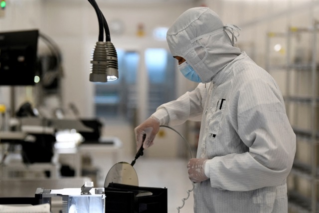
Why it matters: Testing isn’t optional. A 2nm chip flops without 99.999% yields; one bad handler, and you’re scrapping millions. ASE’s Renwu play — phased buildout to 2029 — promises automation that slashes defect escape rates, leaning on AI-driven adaptive testing (they hint at it, anyway).
Sprawling thought: Imagine handlers that learn from each wafer, predicting failures via ML models trained on petabytes of historical data — that’s the shift, from static scripts to dynamic verification, mirroring how NVIDIA’s CUDA evolved GPU programming. ASE isn’t saying it outright, but partners like HTA specialize in exactly that robotic intelligence.
Skepticism creeps in. $3.4 billion? Huge for OSAT, peanuts next to TSMC’s $40B annual capex. And talent wars — Taiwan’s engineers are gold; poach too many from fabs, and someone starves.
Yet. Bold prediction: By 2030, Renwu becomes the de facto hub for AI chip sign-off, pulling AMD, Broadcom closer while US efforts lag on cost.
WinWay brings the electrical guts — high-pin-count testers for HBM stacks. HTA? Precision automation, think sub-micron placements under 24/7 duress. Together, they’re wiring a facility that could handle 100,000 wafers monthly at peak.
Why Does Advanced Testing Suddenly Demand $3.4 Billion Facilities?
Chips evolved. Gone are monolithic dies; enter heterogeneous integration — logic + memory + photonics, all screaming for multi-modal tests: RF, power integrity, even quantum noise floors.
ASE gets it. Their Kaohsiung expansions already hum with System-in-Package validation, but Renwu scales it for exascale era. (Parenthetical: Exascale? Think Frontier supercomputer on steroids, but in your phone.)
Conversational pivot: So, developers — yeah, you — rejoice. Faster testing cycles mean quicker tape-outs, less respins. But fabs? They’ll grumble at OSAT pricing power.
Historical parallel I see nowhere else: This mirrors Applied Materials’ 1990s metrology boom. Back then, 0.25um nodes needed new inspection paradigms; today, angstrom-scale testing demands Renwu-scale bets. ASE’s ahead, but only if they nail software stacks.
Dense wrap: Execution risks loom — supply chain snarls for rare probes, power hikes from Taiwan’s grid strains, plus that ever-present quake shadow. Still, if they pull it off, OSAT margins jump 5 points easy.
One sentence: Taiwan digs in.
🧬 Related Insights
- Read more: Sony’s PS5 Price Surge: AI Memory Crunch Hits Consoles Hard
- Read more: Intel Wakes a Raccoon-Haunted Fab to Chase Packaging Gold
Frequently Asked Questions
What is ASE’s Renwu advanced testing project?
ASE Test’s $3.4B facility in Renwu Industrial Park focuses on validating advanced nodes like 2nm and complex packages for AI chips, partnering with WinWay and HTA.
How will ASE’s Renwu investment impact semiconductor supply chains?
It bolsters Taiwan’s testing dominance, potentially speeding yields for global chipmakers while hedging US-China risks.
When will ASE’s Renwu testing site be operational?
Phased rollout starts 2027, full capacity by 2029.