A single chip, smaller than a grain of sand, humming with the potential of a thousand future innovations. That’s the promise etched into the silicon Intel is currently dreaming up, not for tomorrow, but for the world a decade from now.
Look, this isn’t just about Intel playing catch-up or boasting about smaller numbers. This is about the fundamental architecture of computing itself, a platform shift as profound as the transition from vacuum tubes to transistors. Intel’s announcement that they’ve already kicked off development on their 10A and 7A fabrication technologies – successor nodes to the upcoming 18A and 14A – isn’t just corporate speak; it’s a declaration of intent. They’re not just building chips; they’re sculpting the very building blocks of the digital age for years to come.
Imagine a bustling city. Right now, we’re marveling at the gleaming skyscrapers of the 18A and 14A, the latest marvels of engineering. But Intel’s CEO, Lip-Bu Tan, is telling us they’ve already hired the architects and surveyed the land for the districts that won’t even break ground for another five, maybe seven years. That’s the kind of foresight we’re talking about. It’s a marathon, not a sprint, and Intel is clearly lining up for the long haul.
Here’s the thing: this kind of long-range planning isn’t just good business; it’s essential for survival. As Tan himself articulated, companies don’t just buy products; they buy into roadmaps, into the promise of a stable, innovative partner for the long haul. When you’re talking about the foundational technologies that power everything from your smartphone to global data centers, stability and a clear vision of the future are worth more than gold. Intel knows this, and they’re betting on it.
The Holy Grail of 14A: PDK Promises and Partner Trust
Before we leap too far into the future, though, there’s the immediate, glittering prize: the 14A node. Development is chugging along, right on schedule. The v0.5 Process Design Kit (PDK) is already out there, letting early adopters poke and prod, to test the waters and see what’s possible. But the real magic, the “Holy Grail” as Tan calls it, is the v0.9 PDK. Its arrival in October is more than just a technical milestone; it’s the handshake, the firm commitment to customers that Intel is ready to deliver. This isn’t just about having the technology; it’s about building the trust that partners will entrust their most critical designs to Intel’s fabs.
“The Holy Grail is v0.9 PDK. Right now, we are looking at October to [hand it to] the outside customer. Internal customer will be earlier, so that we make sure that we really clean the pipe, make sure that we are doing right, make sure that we can sell with good quality.”
And the buzz is real. Multiple customers are already circling, defining what their future products will look like, where they’ll be manufactured, and what kind of capacity they’ll need. Intel, wisely, isn’t naming names yet – that’s a dance best choreographed with the customers themselves. But the engagement is undeniable. This 14A node, with its backside power delivery capabilities for high-end processors, is shaping up to be a significant player, even as TSMC also eyes its own A14 node around the same time.
Why High-NA EUV is the Next Big Leap
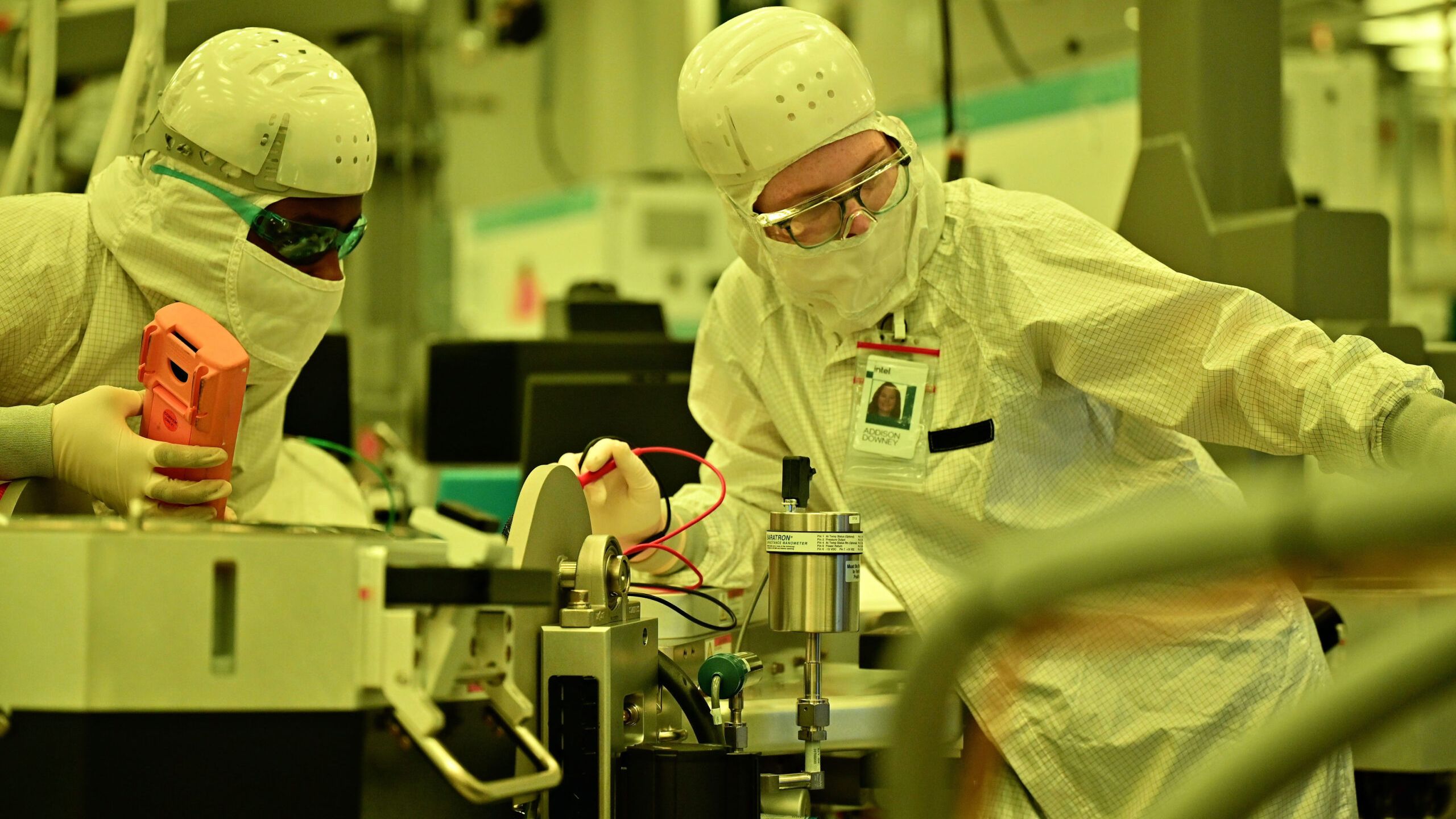
The real game-changer, the thing that makes 14A and the future nodes genuinely exciting, is the integration of High-NA EUV lithography. This isn’t just an incremental upgrade; it’s like upgrading from a whisper-quiet electric car to a supersonic jet. High-NA EUV allows for the etching of even finer, more complex patterns onto silicon wafers. But it’s not a simple plug-and-play. This technology demands a whole new ecosystem: new photoresists, new masks, new metrology, new design rules – the works. Intel is working hand-in-hand with ASML, the undisputed king of EUV, and its partners to ensure this complex symphony of innovation plays out flawlessly.
Will this new tech make my current chip obsolete?
Not overnight, no. Technology adoption is a process. While Intel’s 10A and 7A represent the future, consumer devices and even many enterprise solutions will continue to rely on older, more established nodes for years to come. Think of it like how we still use older models of cars – they work perfectly well for their intended purpose. However, the cutting edge will rapidly adopt these new processes for performance-critical applications like advanced AI and high-performance computing.
When can I actually buy a chip made with 10A or 7A?
That’s the million-dollar question! We’re talking about the development of 10A and 7A technologies now, with roadmaps for the next decade. The 14A node, which is much further along, is slated for risk production in 2028 and volume production in 2029. The 10A and 7A will come significantly after that, likely in the early to mid-2030s for widespread availability, depending on the pace of development and the ecosystem’s readiness.
What’s the difference between Intel’s 14A and TSMC’s A14?
While they share a number, they’re not direct competitors in every aspect. Intel’s 14A is engineered with backside power delivery, making it particularly well-suited for high-end data center processors. TSMC’s A14 is also an advanced node, but the specific architectural choices and target markets can lead to different strengths and performance characteristics. Plus, Intel’s 14A is positioned to be one of the first to use High-NA EUV for high-volume manufacturing, a significant technological differentiator.