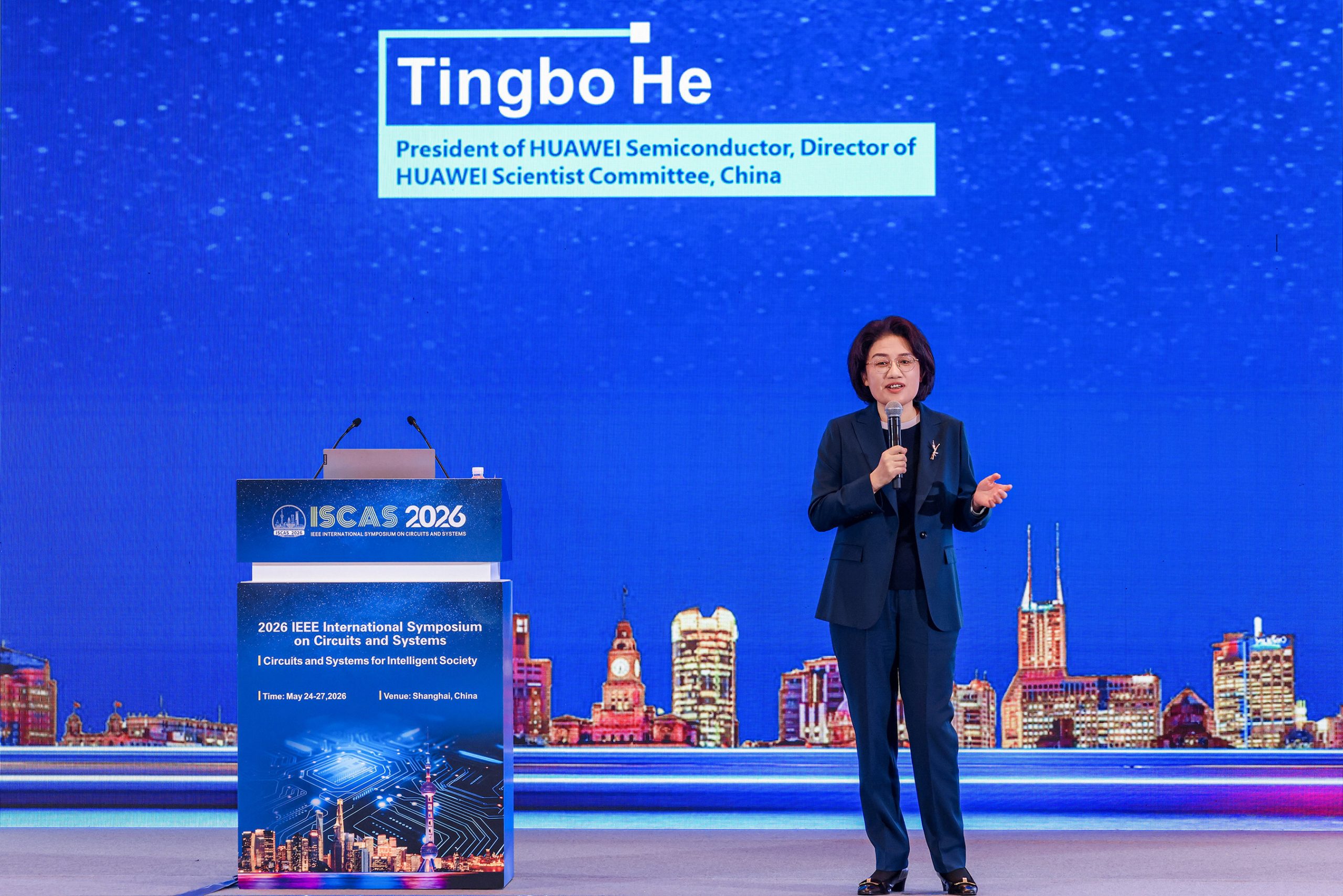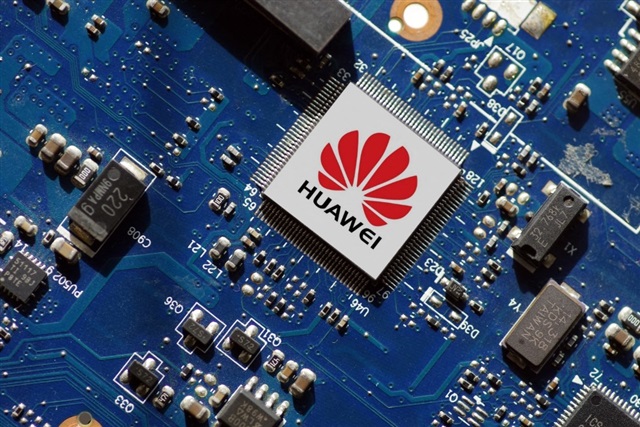
Did you even know you were waiting for a new way to measure silicon? I mean, we’ve all just… accepted it. Moore’s Law. Transistors getting smaller, chips getting faster. It’s been the gospel for decades. But what if that gospel is gospel no more? What if the choir is singing a different tune, a tune that sounds suspiciously like… Huawei’s new “Tau (τ) Scaling Law”? Unveiled at ISCAS 2026, this isn’t just some minor firmware update or a slightly shinier die. This is China planting a flag, yelling “New game in town!” and fundamentally challenging the bedrock of semiconductor evolution. And frankly, it’s exhilarating.
Think of it like this: for years, we’ve been measuring car performance by 0-60 mph times. Pure speed. But what if the world’s road conditions changed? What if traffic became a constant, and you needed cars that could navigate dense urban jungles, optimize fuel efficiency in stop-and-go, and maybe even… predict the traffic lights? Suddenly, 0-60 doesn’t tell the whole story, does it? Huawei’s Tau Law is that shift. It’s a recognition that simply cramming more transistors onto a chip, the old way of the highway, might be hitting a dead end. They’re proposing a new yardstick, one that values efficiency, intelligent resource allocation, and perhaps a more holistic view of performance in the complex, AI-driven world we’re rapidly building.
This move by Huawei is nothing short of a declaration of independence from the tyranny of the shrinking transistor. It’s like a chef who, tired of chasing ever-finer grains of salt, decides to invent a whole new spice blend that transforms the dish entirely. They’re not just tweaking the recipe; they’re creating a new culinary philosophy. China, facing the brunt of global semiconductor restrictions, has been pouring resources into its domestic chip industry. This isn’t just about catching up; it’s about creating their own path forward, a path that might just leave the rest of the world playing catch-up in a different race altogether.
Is This Just PR Smoke and Mirrors?
I’ll admit, my first thought was, “Here we go. Another tech giant trying to spin a narrative.” But the depth of the research, the specific metrics they’re proposing with Tau Law—it feels like more than just a marketing ploy. They’re talking about measures that capture the interplay between hardware architecture, software optimization, and the actual computational tasks. This isn’t about smaller in the traditional sense, but smarter. It’s a move that acknowledges that future performance gains will come from the intelligence within the chip and how it interacts with its environment, not just its raw transistor count. It’s a bold, almost defiant, pivot.
What’s truly fascinating here is the timing. As the West grapples with the limitations of traditional scaling and the immense power demands of AI, Huawei is proposing a paradigm shift. This could very well be the intellectual property that unlocks the next wave of computational power, and if they can successfully embed this thinking into their manufacturing and design ecosystem, they could leapfrog established players. It’s the digital equivalent of a nation discovering a new fundamental force of physics and building its entire technological infrastructure around it.
Huawei believes traditional metrics are no longer sufficient to capture the complexity and efficiency of modern computing workloads, especially those driven by AI. The Tau Scaling Law aims to provide a more comprehensive and forward-looking approach to measuring semiconductor progress.
This pivot is also a masterclass in strategic diversification. While the world obsesses over nanometer counts, Huawei is building a new engine. Imagine the impact if other nations and companies adopt this. It would mean a bifurcation of the semiconductor roadmap, with two distinct sets of standards and optimization targets. The implications for the global supply chain, for R&D investment, and for the very definition of what a “high-performance chip” is, are immense. We’re not just talking about new chips; we’re talking about a new language for computing.
Why Does This Matter for the Future of AI?
This isn’t just about faster processors for your phone or laptop. This is about AI. AI models are getting monstrously complex, and their hunger for computational power is insatiable. If the old scaling laws are slowing down, and if new metrics like Tau Law can unlock more efficient, more capable AI processing, then this is the next frontier. It’s the difference between trying to build a skyscraper with increasingly tiny bricks versus discovering a new, incredibly strong and lightweight building material. Huawei isn’t just building a better brick; they’re proposing a whole new architectural principle. And when you’re talking about powering the next generation of artificial intelligence, that’s not just an improvement; that’s a revolution waiting to happen.
The old ways are like trying to make a steam engine run on electricity—you’re fundamentally misaligned. Huawei’s Tau Law is an acknowledgment that the silicon roadmap needs a reboot. It’s an audacious move, a proof to their R&D prowess and their strategic foresight in a geopolitical landscape that forces innovation. They’re not just adapting; they’re leading the charge toward a new definition of what’s possible in computing. And that, my friends, is a story worth watching with wide, wonder-filled eyes.