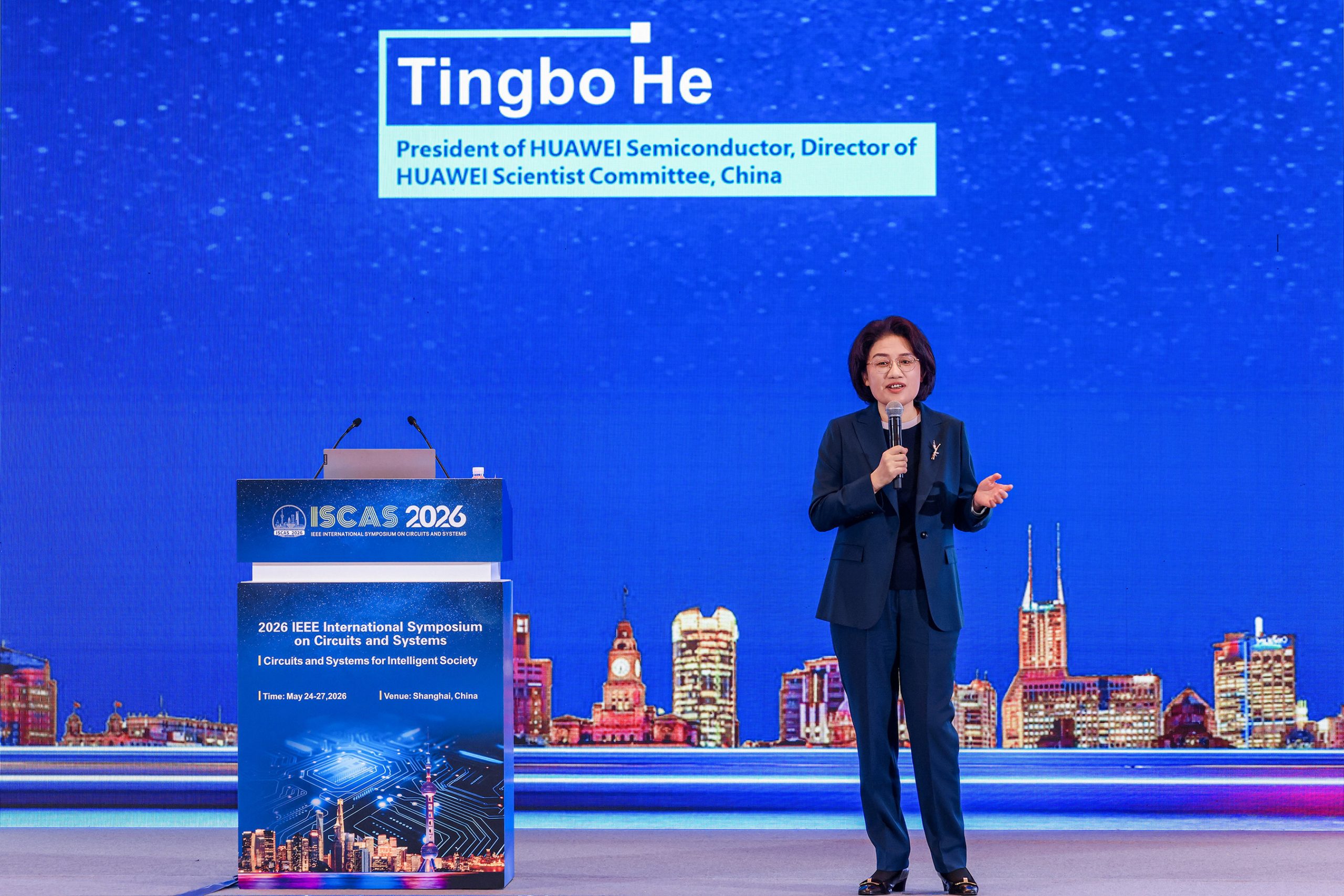
The hum of servers, the glow of monitors, the very pulse of our digital world — it’s all powered by silicon. And right now, that pulse is speeding up, thanks to a seismic announcement from Huawei. Forget the incremental march of Moore’s Law; we’re witnessing a full-blown sprint. He Tingbo, a Huawei board member and the maestro behind HiSilicon, stepped onto a stage in Shanghai and, with every word, detonated a new paradigm in chip architecture. This isn’t just about making smaller chips; it’s about making them smarter, faster, and entirely on their own terms. The era of being beholden to Western manufacturing has just been put on notice.
Here’s the thing: the world of semiconductors operates on a delicate dance of physics and economics. For years, the mantra has been shrink, shrink, shrink. We’ve squeezed transistors down to astonishing sizes, chasing ever-higher densities. But that path, while fruitful, hit a wall for Huawei, thanks to global sanctions. Access to the cutting-edge Extreme Ultraviolet (EUV) lithography machines — the super-precise tools needed for the most advanced shrinking — became a no-go. It was like telling a concert pianist they couldn’t use their favorite grand piano. A dead end, right? Wrong. For Huawei, it was a catalyst.
The LogicFolding Revolution
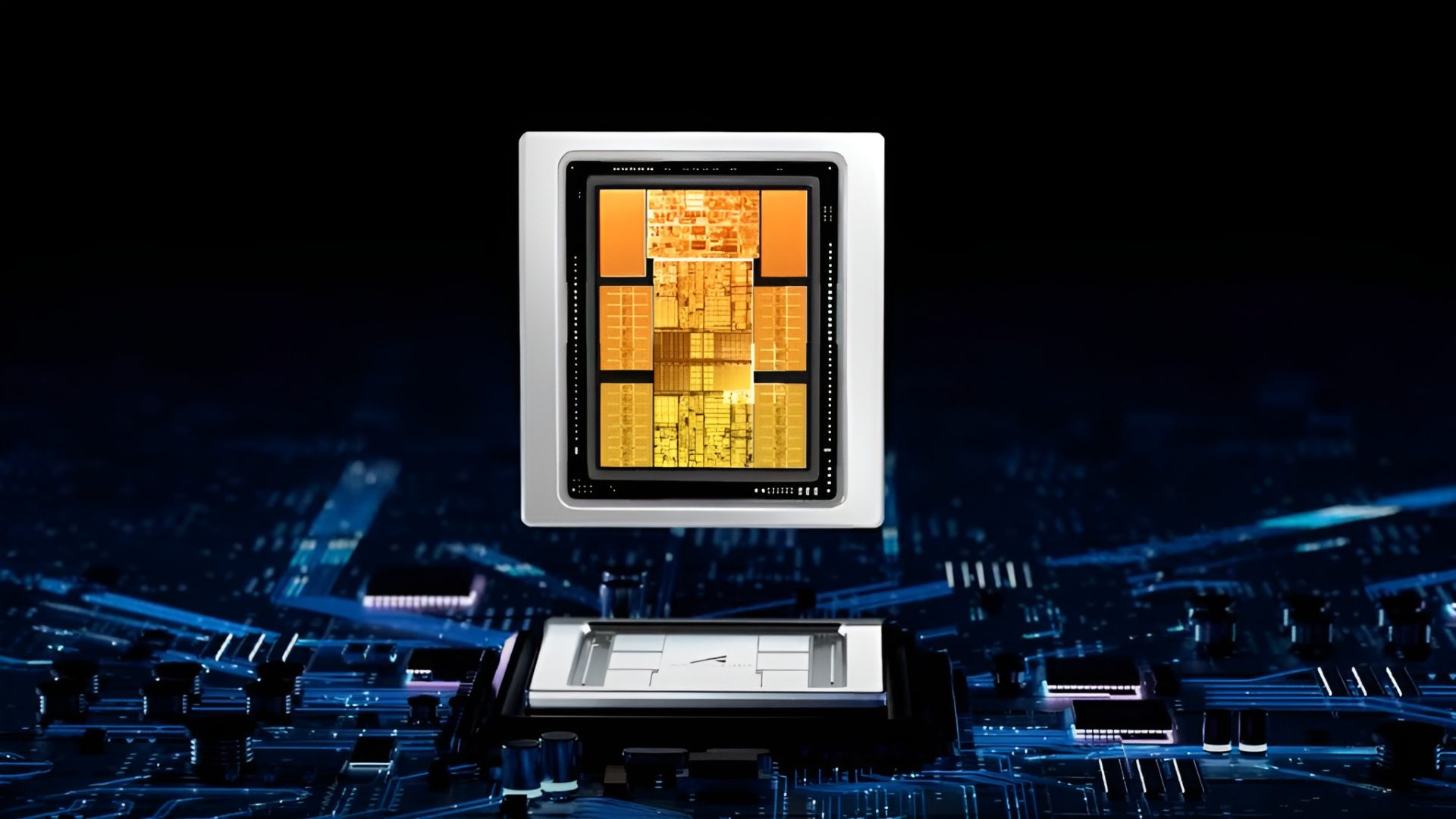
Instead of lamenting the tools they couldn’t have, Huawei decided to invent new tools, or rather, a new way of thinking about the tools they did have. Enter ‘LogicFolding.’ Imagine, if you will, taking a complex electrical circuit, usually spread out like a sprawling city, and instead, folding it, stacking it, creating a multi-story metropolis where pathways are drastically shorter. That’s LogicFolding. It’s a physical re-imagining of chip architecture, essentially creating a dual-layer framework that tucks logic circuits closer together. The payoff? A staggering 55% increase in transistor density and a 41% leap in power efficiency. This isn’t just a clever hack; it’s a fundamental architectural rethink that allows them to achieve remarkable performance without needing those elusive EUV machines. It’s like finding a shortcut through the mountains instead of trying to tunnel through them.
Huawei’s alternative path means China can dramatically close the performance gap by packaging and structuring chips differently — significantly mitigating the impact of the US clampdown.
But LogicFolding is only part of the equation. It’s built upon a new theoretical foundation, Huawei’s ‘Tau Scaling Law.’ While Moore’s Law was all about physical size, Tau Law is about temporal optimization. It’s about how fast data can flow through the system. Think of it like a superhighway versus a winding country road. Shrinking transistors is like making the road surface smoother. Tau Scaling is about adding more lanes and optimizing traffic flow to get you there faster, regardless of how narrow the road might have been initially. It’s a shift from density through miniaturization to density through optimized data velocity. This is, for me, the truly exciting part – a fresh philosophical approach to chip design that could redefine what we even consider when we talk about ‘next-gen’ processors.
Why Does This Matter for AI Development?
This isn’t just about snazzier smartphones, though the Kirin chips hitting Huawei’s flagship Mate 90 series this autumn will certainly bring that. The real prize, the ultimate frontier Huawei is targeting, is AI. Their sights are set on scaling LogicFolding to their Ascend AI processors and massive data center clusters by 2030. Why is this a big deal? Because the insatiable hunger of AI for computational power is the defining characteristic of our age. Training complex models, running inference at scale – these tasks demand immense processing capabilities. Right now, companies like Nvidia are the undisputed kings of this hill, powered by their own advanced silicon. Huawei’s announcement suggests they’re not just aiming for a seat at the table; they’re building their own banquet hall. By 2031, they confidently project designing chips with a transistor density equivalent to a 1.4nm process. That’s practically science fiction territory, achieved through a fundamentally different pathway. This could mean more powerful, more energy-efficient AI hardware, built domestically, disrupting the current geopolitical landscape of chip supply.
Is Huawei’s New Chip Architecture a True Moore’s Law Killer?
Moore’s Law isn’t dead, but it’s certainly been put on notice by Huawei’s ingenuity. The beauty of the Tau Scaling Law and LogicFolding is that they’re not trying to replace the fundamental physics of shrinking transistors. Instead, they’re offering an alternative, and potentially complementary, route to enhanced performance and density. It’s like realizing you can build taller skyscrapers even if you can’t dig the foundations any deeper. The existing infrastructure of chip manufacturing might not be directly applicable to EUV-less production at the bleeding edge, but Huawei’s announcement signals a potential divergence. They’re creating a parallel path to high performance, one that is less reliant on the specific choke points of international supply chains. This will undoubtedly spur further innovation in advanced packaging and chiplet technologies globally as others scramble to understand and replicate these principles.
So, what’s the takeaway? We’re at the dawn of a new age in chip design. Huawei, facing immense pressure, has responded not with a whimper, but with a roar of innovation. They’ve taken a constraint and turned it into an opportunity, forging a new path forward. The implications for the future of computing, especially in the AI domain, are immense. The race is on, and the finish line just got a whole lot more interesting. This is the kind of bold engineering that electrifies the future.