For engineers and scientists grappling with the messy reality of materials – the defects, the interfaces, the unpredictable nature of alloys – the implications are profound. It means moving beyond idealized theoretical models and into simulations that mirror the actual performance and behavior of the materials we rely on. Think better batteries, more efficient solar cells, and ultimately, more predictable and reliable next-generation electronics.
It’s always been a bit of a dance, hasn’t it? You want your computer models to accurately predict how a material will behave, but the more atoms you cram into the simulation, the longer it takes to get an answer. This forces a constant compromise: sacrifice realism for speed, or vice-versa. For decades, this computational bottleneck has meant that many of the most interesting and important material properties – those arising from imperfections, impurities, or complex structures – remained tantalizingly out of reach for accurate, first-principles simulation.
As George E. P. Box famously quipped, “All models are wrong, but some are useful.” The problem was that the ‘useful’ models for real-world materials were often too computationally expensive to be practical, and the ‘fast’ models were too simplistic to be truly predictive.
Historically, a simple crystal could be simulated by repeating a small unit cell. This works for predicting bulk properties of perfect materials, but real-world applications rarely involve perfect crystals. Surface defects, grain boundaries, and alloy variations are often the very things that dictate a material’s failure or success. Ignoring these complexities meant simulations might miss the critical behaviors engineers needed to understand.
In the past, the solution was to simplify. Instead of treating atoms with quantum mechanics, researchers might resort to classical physics, essentially treating them as billiard balls. This saves immense computing power but severely limits the accuracy and transferability of the results. It’s like trying to understand fluid dynamics by only watching water flow down a drain – you get a general idea, but you miss the nuances of turbulence.
And then there’s temperature. Standard Density Functional Theory (DFT), a workhorse of atomistic modeling, is fundamentally a zero-temperature approach. Accounting for thermal vibrations or dynamic processes requires indirect methods, often necessitating even larger simulation cells to capture long-wavelength phonon modes without distorting the physics. This, again, slams into the computational wall.
Plane-wave DFT, while incredibly successful for periodic crystals, falters when periodicity breaks down. Defects, surfaces, amorphous structures, and random alloys all demand larger simulation cells, pushing computational costs sky-high. It’s here that techniques based on a linear combination of atomic orbitals (LCAO) have offered a more natural fit. Because the basis functions are tied to atoms, they handle interfaces and vacuum regions more gracefully, and generally use fewer basis functions per atom, which should make larger calculations more feasible.
But the fundamental scaling problem of DFT – its computational cost increasing steeply with system size – still looms large. Faster hardware, like GPUs, has been a godsend, accelerating calculations by orders of magnitude and bringing simulations that once took weeks down to hours. Yet, even with these advancements, the scaling law itself hasn’t been rewritten. We’re still wrestling with the core mathematical challenge of simulating millions, let alone billions, of atoms with the required accuracy.
This is where the real innovation is happening. The industry is moving beyond just faster hardware to fundamentally new algorithms. The promise lies in methods that avoid the most computationally intensive parts of standard DFT. While some linear-scaling methods exist, they often sacrifice local, chemically detailed information for global properties like total energy. That’s not always what an engineer needs when troubleshooting a specific failure mechanism.
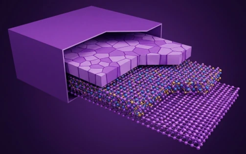
The Machine Learning Advantage in Atomistic Modeling
Here’s the exciting part: machine learning (ML) is poised to change the game. By training physics-informed graph neural networks to predict components of the DFT solution directly from atomic structure, researchers can drastically cut down compute time. This isn’t just an incremental speed-up; it’s a change in the scaling of the problem. Instead of calculations scaling cubically with system size (O(N³)), ML-DFT approaches aim for linear scaling (O(N)).
This shift could unlock simulations of systems with millions of atoms, preserving access to those crucial local properties that are essential for understanding material behavior at the atomic level. Imagine simulating the diffusion of dopants in a semiconductor at an unprecedented scale, or accurately modeling the complex interfaces in a next-generation battery electrode. Companies like QuantumATK are already integrating these ML-DFT techniques into their platforms, making them more accessible and practical, especially when coupled with the power of GPUs.
Why Does This Matter for Real-World Applications?
It means the gap between theoretical prediction and experimental reality is narrowing. For materials scientists and engineers, this translates to:
- Accelerated Discovery: New materials with specific desired properties can be identified and validated much faster.
- Predictive Reliability: Simulations can more accurately predict how materials will perform under real-world conditions, including defects and temperature.
- Cost Reduction: Designing and testing materials virtually reduces the need for expensive and time-consuming physical prototypes.
This isn’t just an academic exercise; it’s a direct path to innovation across numerous industries, from renewable energy and advanced manufacturing to pharmaceuticals and aerospace.
So, while the journey towards perfect atomistic simulation is ongoing, the move toward scale and realism driven by ML and advanced algorithms marks a significant inflection point. It’s about finally being able to simulate the world as it truly is, not just how we wish it were.