India’s Semiconductor Ambition Takes Root.
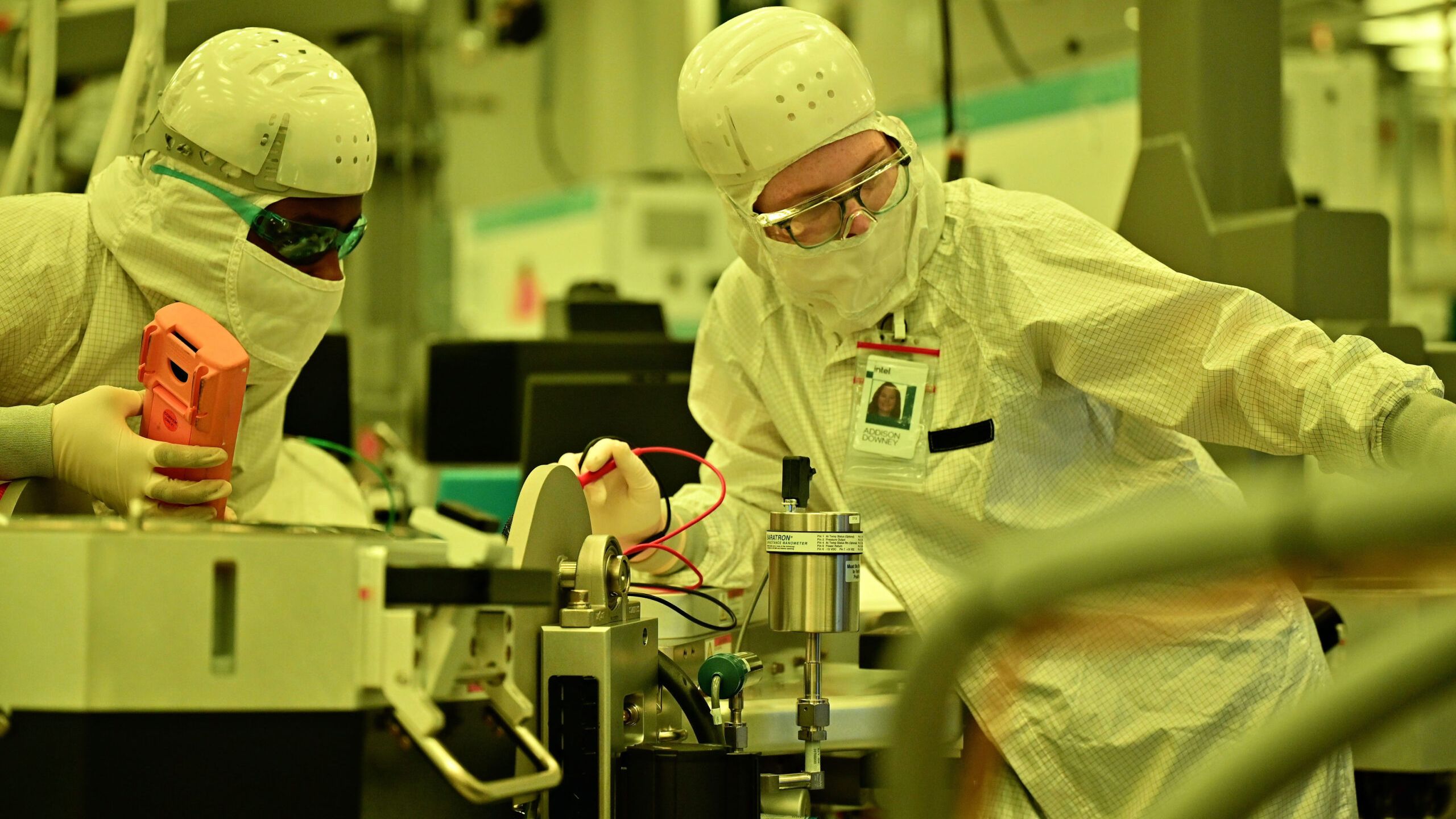
ASML’s lithography tools are heading to India. It’s not a drill. This announcement, inked during Prime Minister Narendra Modi’s Netherlands visit, places the Dutch lithography giant’s gear squarely within Tata Electronics’ ambitious Dholera fabrication plant. This isn’t just about equipping a facility; it’s about seeding India’s first attempt at true, front-end semiconductor manufacturing. The deal, a memorandum of understanding, covers not only the state-of-the-art lithography machines but also vital talent development and supply chain integration – the nuts and bolts required to go from zero to silicon. And let’s be clear, India’s semiconductor sector has been at zero for front-end wafer fab capacity. Until now.
Nodes of Significance
The Dholera fab, a sprawling 300mm facility, isn’t aiming for the bleeding edge of semiconductor technology just yet. Taiwan’s Powerchip Semiconductor Manufacturing Corporation (PSMC) is licensing process technology for nodes ranging from 28nm down to 110nm. This isn’t the 3nm or 5nm process that fuels the latest flagship smartphones, but it’s precisely where the bulk of the world’s chips are still made – think automotive, industrial, and many consumer electronics applications. Targeting 50,000 wafers per month, this output aims to serve power management ICs, display drivers, microcontrollers, and high-performance computing logic, touching automotive, mobile, AI, and communications markets. It’s a strategic starting point, not a leap into the most complex nodes immediately.
ASML’s deep expertise in holistic lithography solutions will ensure the timely ramp of our fab in Dholera, create a resilient and trusted supply chain for our global customers, drive innovation, and develop talent locally.
ASML’s CEO and MD, Randhir Thakur, Tata Electronics
Financial Underpinnings and Ground Realities
This isn’t a shoestring operation. The Dholera project represents a staggering $11 billion investment, with India’s government shouldering 50% of eligible costs via the India Semiconductor Mission. The Gujarat state government is adding further incentives – subsidized land, reduced power tariffs, stamp duty exemptions – sweetening the pot considerably. It’s a clear indication that New Delhi views domestic chip manufacturing not as a nice-to-have, but as a strategic imperative for national security and economic growth. Interestingly, the project has already faced its own engineering hurdles; civil construction is around 50% complete, but a significant redesign was necessary late last year due to challenging soil conditions – soft and saline ground requiring structural modifications. Yet, the companies maintain this won’t derail the timeline, with trial production still eyed for later this year.
Why Does This Matter for India’s Global Standing?
India’s entry into front-end chip fabrication is a geopolitical statement as much as an economic one. For decades, the nation has been a consumer of chips, albeit a massive one, and a powerhouse in chip design and assembly/testing. This Dholera fab, however, aims to change that equation fundamentally. By joining initiatives like the U.S.-led Pax Silica alliance, India signals its intent to become a more integrated and self-sufficient player in the global semiconductor supply chain. The absence of domestic front-end capacity has always been a glaring gap, and this move addresses it head-on. While Micron already operates an assembly and test facility in Gujarat, the Dholera foundry is the sole commercial venture aiming for the complete wafer fabrication process.
The ASML Factor: A Necessary Enabler
ASML’s involvement is, frankly, non-negotiable for any nation serious about advanced semiconductor manufacturing. Their lithography machines are the heart of the chipmaking process, the incredibly complex instruments that etch complex patterns onto silicon wafers. Without ASML, building a competitive fab is simply not possible. Their presence in Dholera signals a level of commitment and technological transfer that goes beyond mere equipment sales. It suggests a long-term partnership, aimed at building indigenous capability. ASML CEO Christophe Fouquet’s remarks about India presenting “many compelling opportunities” and looking forward to contributing “technological expertise” and helping “nurture talent” are more than just corporate platitudes; they are acknowledgments of India’s growing importance in the global tech landscape and ASML’s role in that ascent.
Is this too little, too late for India?
It’s easy to be cynical. India is decades behind the established semiconductor manufacturing hubs of Taiwan, South Korea, and the United States. The Dholera fab’s focus on mature nodes, while pragmatic, doesn’t immediately position India to compete at the absolute leading edge. However, to dismiss this as a mere footnote would be a mistake. This is about establishing a foundational capability, building an ecosystem, and demonstrating national will. Think of it as India laying the cornerstone for a future skyscraper. The initial structure might not be the tallest or the most complex, but it’s the essential first step. The real test will be in the execution, the scaling, and the ability to attract further investment and technological advancements as the global chip industry continues its relentless march forward. The foundations are being laid, and ASML’s presence is a strong endorsement of that effort.
🧬 Related Insights
- Read more: Tiny Photonic Chip Projects Mona Lisa on a Sand Grain – Quantum Fix or Lab Toy?
- Read more: IQE Secures £81m Boost: A Lifeline or Just Another Chapter?
Frequently Asked Questions
What is the Dholera chip fab’s target production capacity?
The Dholera fab is designed to produce 50,000 wafers per month at full capacity.
What types of chips will the Dholera fab produce?
It will focus on chips for power management ICs, display drivers, microcontrollers, and high-performance computing logic, targeting automotive, mobile, AI, and communications applications.
Will ASML’s equipment be used for advanced chip nodes in India?
Initially, the Dholera fab will utilize PSMC’s licensed technology for nodes ranging from 28nm to 110nm, which are considered mature but crucial for many applications, rather than the most advanced nodes.