Picture this: the chip world buzzing with hype around nanosheet transistors finally hitting mass production, TSMC and Intel flexing identical SRAM cells, everyone patting themselves on the back for cracking Moore’s Law one last time. That’s what we all expected — a tidy progression, sub-2nm nodes locked in, AI servers guzzling power without a hitch. But 2025? It flipped the script. These top semiconductor stories reveal not just gadgets, but the gritty, decades-long grind from wild lab sketches to fab floors — and the bureaucratic landmines that can derail it all.
Look, I’ve chased silicon tales for years, and this year’s haul feels like a throwback to the 1950s transistor scramble: pure chaos masked as progress.
Diamonds Don’t Just Cool Your Drink — They Chill Transistors Too
Stanford’s Srabanti Chowdhury drops a bombshell: grow diamonds — yes, actual diamond crystals — nanometers from scorching transistors. Her team’s radio gadgets ran 50°C cooler. It’s not bling; it’s a heat war chest for 3D-stacked chips.
“Stanford professor Srabanti Chowdhury explained how her team has come up with a way to grow diamonds inside ICs, mere nanometers from heat-generating transistors. The result was radio devices that were more than 50 degrees Celsius cooler, and a pathway to integrate the highly heat-conductive material in 3D chips.”
But here’s my take — and it’s one IEEE Spectrum glossed over: this echoes the 1980s gallium arsenide push, where killer demos (faster, hotter-running RF chips) crashed against scaling woes. Diamonds? Thermal conductivity five times silicon’s, sure. Yet integrating CVD diamond growth into a 300mm wafer line? That’s a yield nightmare waiting to happen. Bold prediction: by 2028, it’ll be in niche RF for 6G base stations, not your average GPU.
Short version: heat’s the silent killer in AI datacenters. Diamonds might buy us time.
Why Did ASML’s EUV Laser Saga Feel Like Sci-Fi?
ASML cracks the code on their extreme ultraviolet lithography light source — tin droplets zapped by lasers mimicking supernovas, nods to von Neumann and atomic blasts. Grandfather-grandson lore aside, it’s the ‘how’ that stuns: plasma physics tamed for 2nm nodes.
Everyone banked on EUV as inevitable. But this tale underscores the madness — $200 million machines birthed from decades of dead ends. Shift? Fabs now bet everything on photonics wizardry, not just clever chemistry.
And yet.
China’s 2D flex steals the show: nearly 6,000 molybdenum disulfide transistors in a RISC-V processor, 99.7% yield from lab gear. No billion-dollar cleanrooms needed. That’s the architectural pivot — 2D materials sidestepping silicon’s atomic limits.
Nanoimprint Lithography: Stamping Chips Like Cookies?
Canon’s first nanoimprint system sells — in Austin, no less. Forget EUV’s light tricks; this stamps patterns mechanically. Decades late (I once crashed en route to a startup demo), but viable now.
Is the CHIPS Act Crumbling Before It Builds Anything?
U.S. policy whiplash hits hard. Commerce axes Natcast ($7.4B R&D hub) and SMART USA (digital twins for fabs). Vowed to bridge lab-to-fab? Instead, vitriol kills momentum.
What everyone expected: factories sprouting, China boxed out. Reality: infrastructure choked. My unique spin — this mirrors the 1980s SEMATECH rescue, born from Japan’s DRAM dominance. Back then, it worked because rivals collaborated. Today? Geopolitics poisons the well. Prediction: without fixes, Europe’s imec becomes the real NSTC.
Ouch.
Broadcom and Nvidia shove optical links into switch packages — co-packaged optics for datacenter racks. Low-power, speedy I/O that engineers drooled over for years. Cost and reliability hurdles? Apparently solved.
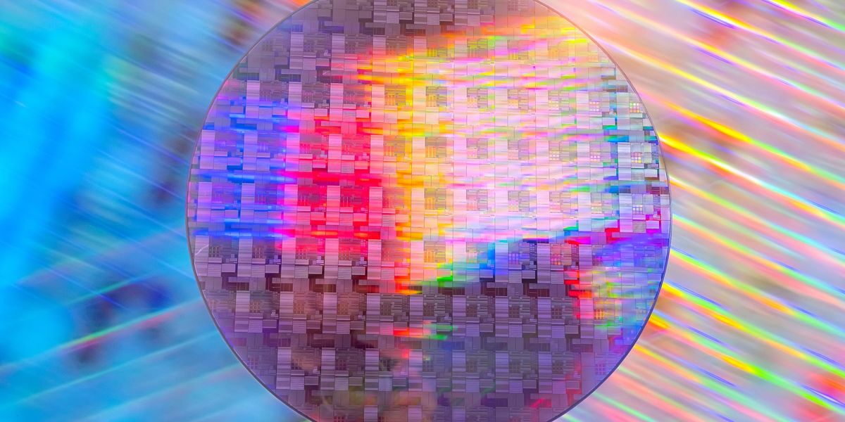
TSMC/Intel nail nanosheet SRAM, pixel-perfect density matches. Synopsys’ FinFET stab lags in speed. The why: gate-all-around wraps channels fully, slashing leakage — but stacking sheets demands etch-precision wizardry.
Why Does the Lab-to-Fab Gap Still Haunt Us?
These stories scream one truth: innovation’s a marathon, not a sprint. Diamonds, imprints, 2D chips — all lab darlings commercializing after 20+ years. EUV? 30. Nanosheets? Evolutionary, not revolutionary.
Underlying shift? Supply chain snarls and policy folly amplify the gap. Fabs cost $20B; labs dream free. CHIPS was supposed to glue them — now it’s glue in the gears.
But optimism flickers. Canon’s stamp could slash EUV bills (no $150k wafers/hour). Optical I/O preps exascale without melting racks. 2D integration hints at post-silicon eras.
Wander with me here — remember Josephson junctions in the ’70s? Hyped for supercomputers, faded fast. 2025’s gems might fare better, or join the graveyard. That’s the thrill.
One-paragraph deep dive: ASML’s tin-plasma dance isn’t just engineering porn; it’s a metaphor for semi’s future. We weaponize star-birth physics for logic gates. Yet Beijing’s 2D RISC-V whispers defiance — low-tech fab sovereignty.
Will 2026 Double Down on These Wins?
Expect diamonds in prototypes, imprints scaling trials. Nanosheets? A14/B0 nodes everywhere. But watch policy — if Commerce doesn’t pivot, U.S. innovation leaks overseas.
Here’s the thing: 2025 exposed cracks. Not doom, but a call to rethink how we midwife tech.
**
🧬 Related Insights
- Read more: Samsung Electro-Mechanics Locks In Crucial Substrates for Nvidia’s Groq 3 LPU Push
- Read more: Optical Metamaterials Swap Cloaks for AI Data Center Speed Demons
Frequently Asked Questions**
What are nanosheet transistors and why now?
Nanosheets stack transistor channels like ribbons, fully gated for better control at sub-2nm. TSMC/Intel hit identical densities in 2025 SRAM — leakage slashed, performance up, but fab complexity skyrockets.
Is nanoimprint lithography replacing EUV?
Not yet — Canon’s first sale stamps cheaper, greener patterns. But EUV’s entrenched for high-volume logic; NIL shines for memory, sensors.
Why did the U.S. kill CHIPS Act centers like Natcast?
Commerce cited mismanagement, sparking backlash. It guts R&D bridges, risking U.S. edge as China fabs 2D chips in labs.