When did we start celebrating people with blowtorches and hunting knives performing surgery on silicon? I ask this because someone, bless their chaotic heart, decided the best way to get a peek at the innards of an Intel Xeon Silver 4110 was to essentially torture it into submission.
This isn’t your daddy’s clean room operation. No, this is the Hackinator’s domain. A place where integrated heat spreaders are pried off with the grace of a medieval dentist and solder bonds are melted with the finesse of a blacksmith. The Xeon was strapped down — literally — to a chopping block. Washers and screws. Because who needs specialized jigs when you have hardware store staples and a disregard for delicate electronics?
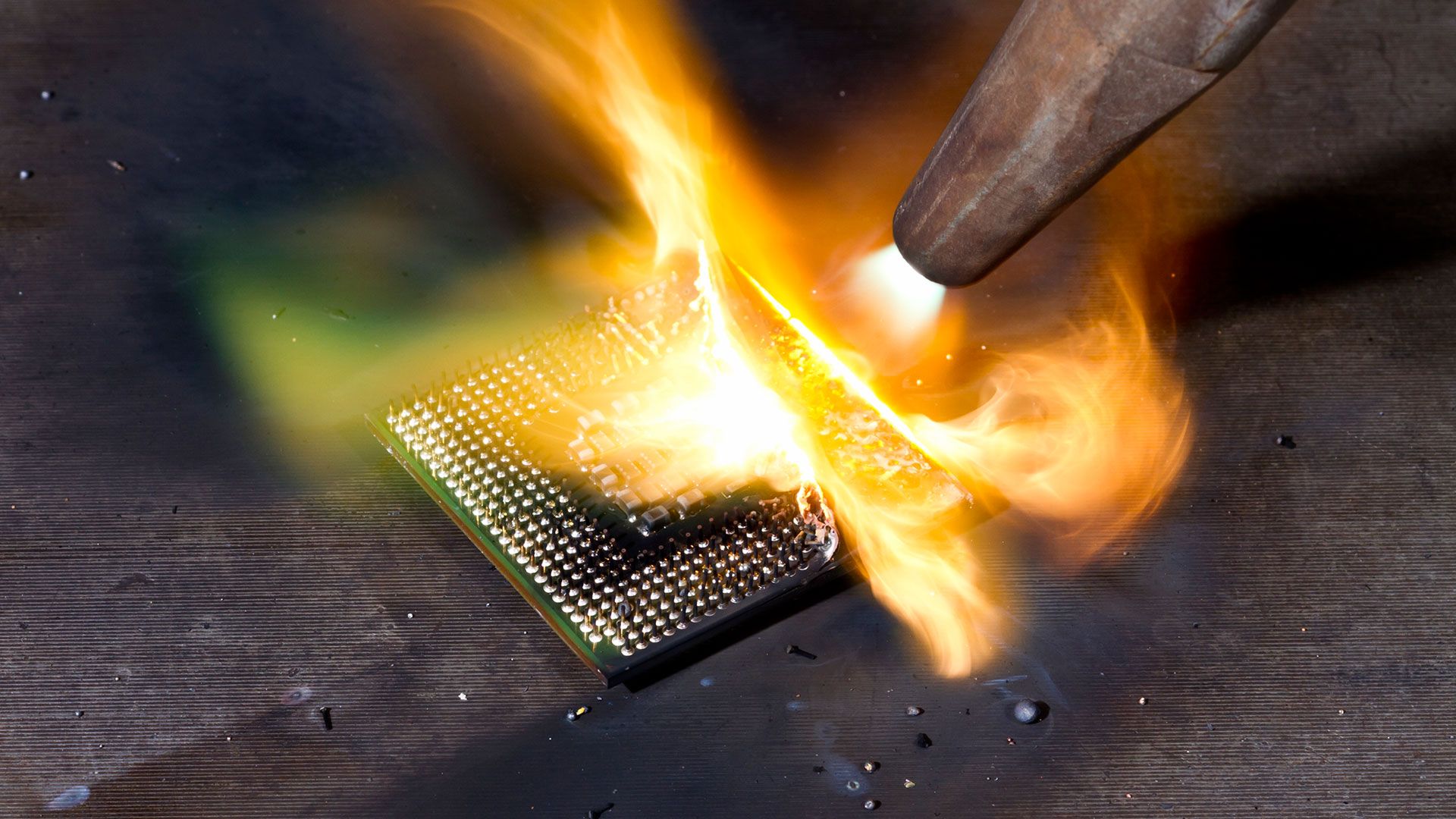
Then the heat gun came out, not for gentle warming, but for what felt like an aggressive pre-game pep talk. Next, the Gerber hunting knife. A tool more at home in the woods than on a circuit board. It’s brutal. There’s no attempt at preservation here. This isn’t about optimizing cooling; it’s about destruction for discovery.
And the IHS? Discarded. Replaced with more screws, more gripping. Because the first round of prying wasn’t enough. Then, the real star of this particular show: the blowtorch. It vaporizes the substrate. Reduces it to ash. All to free a sliver of silicon.
Is this what we’ve come to? After decades of refining micro-lithography and precision engineering, we’re now celebrating destruction? It’s a stark contrast to the clinical, lapping-focused methods we’ve seen before. The usual precision is gone, replaced by brute force and a rather alarming lack of concern for the delicate silicon structure beneath.
With the IHS discarded, the Hackinator adds a metal frame and reapplies grip screws to the substrate before more heating and prying ensues. Eventually, we see the silicon sliver exposed, but it isn’t freed until after a blowtorch is used to decimate the substrate.
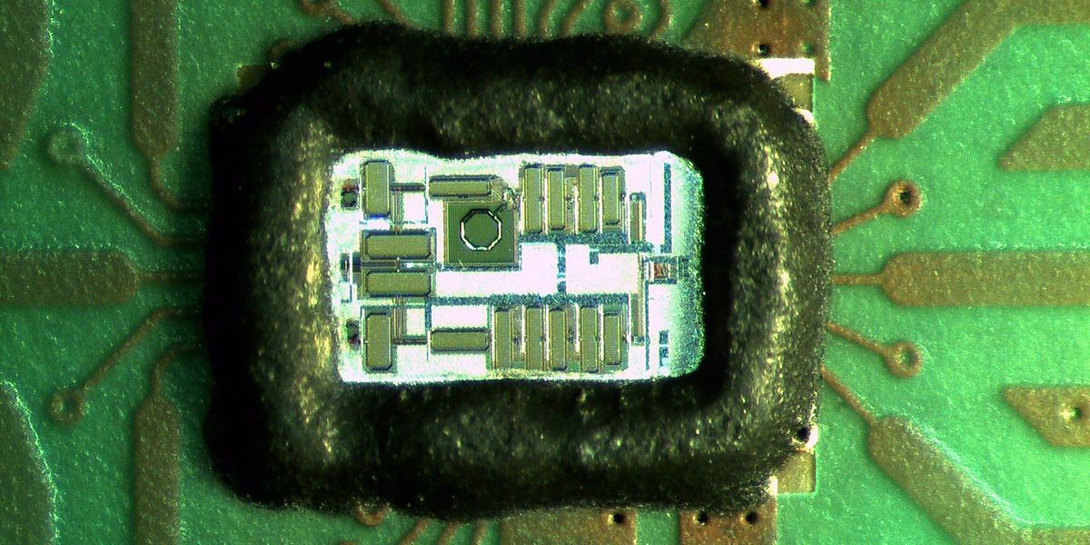
Yet, and here’s the kicker, the resulting close-ups reveal details. Albeit, details marred by the barbaric process. You can see the etched patterns, the complex pathways. It’s like finding a detailed map on a scorched piece of parchment. Far from perfect, certainly not pristine, but somehow, undeniably there.
This whole spectacle begs a question: Are we so desensitized to technological advancement that we need extreme, almost theatrical, methods to feel awe? We’re so used to incremental improvements that a fiery deconstruction of a powerful processor becomes our entertainment. It’s a reminder that sometimes, the most engaging stories aren’t about perfection, but about the sheer, unadulterated audacity of the attempt. The Hackinator isn’t delidding; he’s performing a silicon exorcism.
Why Does This Matter for Chip Enthusiasts?
This isn’t about teaching anyone how to delid their own expensive CPU. Frankly, don’t. Unless you’re prepared for a very expensive and possibly fiery failure. What it does highlight is the raw, underlying architecture of these marvels of engineering. Seeing the bare silicon, even in this violently acquired state, offers a tangible connection to the complex design that goes into every processor. It’s a visceral reminder that behind the marketing and the clock speeds, there’s a physical landscape of transistors and pathways. This method, however questionable, achieves that raw reveal. It’s a crude hammer to a delicate lock, but it does open the door.
Is This the Future of Chip Teardowns?
God, I hope not. The scientific value here is minimal, bordering on nil. The practical application? Zero. It’s pure spectacle. But that’s precisely why it gets clicks. It’s a dare. It’s a middle finger to the carefully controlled world of semiconductor analysis. While clinical, precise methods provide invaluable data for engineers and designers, this kind of chaotic dismantling provides viral content. It’s the difference between a peer-reviewed paper and a TikTok challenge. We’ll likely see more of these sensationalist approaches, not because they’re scientifically valid, but because they capture attention in a crowded digital space.
🧬 Related Insights
- Read more: NVIDIA’s H100 SuperPOD Predicts Millions of Protein Complexes Overnight
- Read more: Intel’s Gaming Shift: Software Over Silicon to Fight AMD’s X3D
Frequently Asked Questions
What does ‘delidding’ a CPU mean? Delidding is the process of removing the integrated heat spreader (IHS) from a CPU, exposing the actual silicon die underneath. It’s often done for better thermal performance by allowing direct contact with a heatsink.
Is delidding dangerous for the CPU? Yes, especially with aggressive methods. Applying too much force, heat, or using incorrect tools can easily damage or destroy the CPU die and surrounding components.
What tools did the Hackinator use? A hot air soldering gun, a Gerber hunting knife, a flat-edged screwdriver, screws, washers, a metal frame, and a blowtorch.