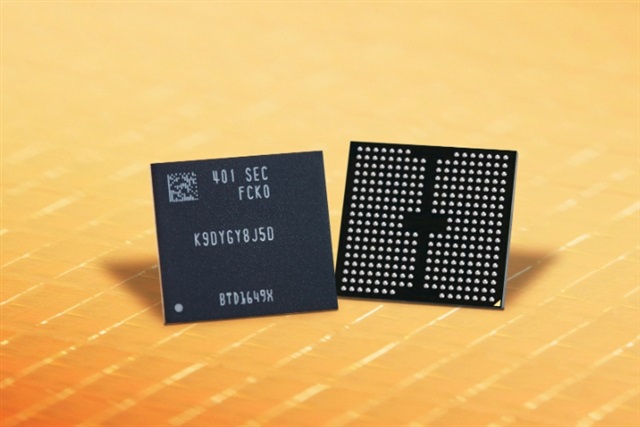
The air in the data center crackled with anticipation, not from a lightning strike, but from the sheer density of information Samsung is now cramming into its latest V-NAND prototype. We’re talking about a 900-layer chip, people! This isn’t just an incremental upgrade; it’s like going from a bungalow to a skyscraper in the world of solid-state drives.
Samsung is doing something truly wild here: they’re essentially strapping two 450-layer cell stacks together. Think of it like building a duplex apartment block by stacking two smaller, perfectly formed buildings on top of each other. This ‘Cell Multi-Bonding’ (CMB) technology is the secret sauce, a clever engineering feat that tackles the once-insurmountable problem of wafer warping and misalignment with fancy ‘Upper Chuck Design’ and ‘Overlay Correction’ tricks. It’s this kind of ingenious problem-solving that makes me so incredibly excited about the future of computing – it’s not just about making things smaller, but about fundamentally rethinking how we assemble them.
We’ve been hearing whispers of 1000-layer NAND for a while now, and this 900-layer beast is the strongest signal yet that it’s not science fiction anymore. This is critical because, in the grand scheme of things, AI hyper-cycles and the insatiable demand for data are creating a veritable digital tsunami. We need storage solutions that can keep pace, and Samsung’s pushing the envelope here is like giving the world an exponentially larger reservoir to hold all that precious information. SSDs, the workhorses of our digital lives – from the servers humming in enterprise data centers to the sleek laptops on our desks and even the smartphones in our pockets – are all going to benefit from this density explosion.
Now, it’s a race, isn’t it? SK Hynix is already rocking the 321-layer club and is pushing for 400. And let’s not forget YMTC in China, which is making serious headway with its own multi-layer NAND designs, investing like mad to boost its output just as the supply-demand gap widens. This competition is healthy; it’s the engine that drives innovation. When companies are locked in a high-stakes battle to push the boundaries of what’s physically possible with silicon, we, the users, are the ultimate winners.
This whole development feels like a direct response to the burgeoning AI revolution. We’re not just talking about faster processors anymore; we’re talking about the infrastructure that feeds those processors with the raw material of data. Imagine AI models trained on datasets so vast they dwarf anything we’ve seen before. To store and access that data efficiently, you need density. This 900-layer V-NAND is like building the super-highways for the AI expressways of tomorrow.
Is Samsung’s 900-Layer NAND Truly Revolutionary?
The ‘revolutionary’ label gets thrown around a lot in tech PR, but this feels genuinely seismic. The sheer act of bonding two separate wafer stacks — each already a marvel of micro-fabrication — into a single, functional unit represents a paradigm shift. It’s not just about cramming more transistors; it’s about a fundamentally different approach to manufacturing, pushing the limits of lithography and 3D stacking to astonishing new heights. This paves the way for 1000-layer NAND, a target Samsung is now visibly inching towards, with aspirations for its release around 2030. While 400+ layer NAND solutions will likely hit the market much sooner, this 900-layer milestone is a powerful statement of intent and capability.
Samsung’s announcement isn’t just about bragging rights in the semiconductor world; it’s a tangible step towards a future where data storage is no longer a bottleneck. It’s about unlocking new possibilities for everything from scientific research and complex simulations to immersive gaming and, yes, the ever-expanding universe of AI. The future of data is vertical, and Samsung just planted a flag at an unprecedented altitude.
Why This Matters for the Future of Computing
Look, we’re living in an age where the sheer volume of data generated daily is mind-boggling. From our social media scrolls to the sensor data flooding in from IoT devices and the massive datasets required for cutting-edge AI, the demand for storage is exponential. Traditionally, we’ve seen improvements in NAND density through making individual layers smaller and more efficient. But we’re hitting physical limits there. Samsung’s CMB approach is like finding a whole new dimension to expand in. It’s a clever workaround, a proof to human ingenuity when faced with seemingly insurmountable obstacles.
This isn’t just about making SSDs a bit faster or a bit bigger. This is about enabling entirely new classes of applications. Think about the scale of data needed to train massive AI models, or the real-time data streams required for autonomous vehicles to operate safely. Without radical increases in storage density and speed, these advancements would be severely hampered, if not impossible. Samsung’s push towards 900-layer and then 1000-layer NAND is, in essence, building the foundation for the next generation of technological leaps. It’s a platform shift, plain and simple.
🧬 Related Insights
- Read more: Metadata Gulps 20% of Supercomputing I/O—GPUs Starve Without New Storage
- Read more: Broadcom’s 400G/Lane DSP: AI’s Bandwidth Savior or Just More Chip Hype?
Frequently Asked Questions
What does Samsung’s 900-layer V-NAND prototype do? Samsung’s prototype achieves 900 layers by bonding two 450-layer NAND flash memory cell stacks into a single device, dramatically increasing data storage density.
When will 1000-layer NAND be available? Samsung is aiming for a release of 1000-layer V-NAND around 2030, with 400+ layer solutions expected in the coming years.
Will this technology make my current SSD obsolete? While this new technology will lead to significantly higher capacity and potentially faster drives in the future, your current SSD will still be functional. However, future storage solutions will offer much greater performance and density.