In 1965, Gordon Moore, co-founder of Intel, published a paper in Electronics magazine with an observation that would define the trajectory of the semiconductor industry for the next six decades. He noted that the number of transistors on an integrated circuit was doubling approximately every year (later revised to every two years) while the cost per transistor was falling. This observation, which became known as Moore's Law, was never a physical law but rather an economic and engineering prediction that became a self-fulfilling prophecy, guiding industry investment and research for generations.
The Golden Era: 1965-2005
For four decades, Moore's Law held with remarkable consistency. Transistor counts doubled roughly every two years, and this scaling delivered a triple benefit: chips became faster (higher clock speeds), cheaper (more transistors per dollar), and more power-efficient (lower voltage per transistor) with each new generation. This triple benefit, sometimes called Dennard scaling after Robert Dennard who formalized the power scaling rules in 1974, drove the explosive growth of the computing industry.
The progression was breathtaking. Intel's 4004 processor in 1971 contained 2,300 transistors on a 10-micrometer process. By 2005, Intel's Pentium D contained 230 million transistors on a 90-nanometer process, a 100,000-fold increase in transistor count and a 111-fold reduction in feature size. Clock speeds rose from kilohertz to gigahertz. The cost of a transistor fell from dollars to fractions of a cent.
This predictable cadence of improvement created a virtuous cycle. Software developers could count on hardware getting faster, so they wrote more ambitious programs. These programs created demand for faster hardware, justifying the billions of dollars in investment needed to develop each new process node. Equipment companies, chip designers, and software developers all aligned their roadmaps to Moore's Law's cadence.
The End of Dennard Scaling: 2005-2015
Around 2005, one of the three pillars of Moore's Law collapsed. Dennard scaling, the principle that power density remains constant as transistors shrink, broke down because of quantum mechanical effects at very small dimensions. Specifically, as transistor gate oxides became thinner, leakage current (current flowing even when a transistor is supposed to be off) grew exponentially, making it impossible to continue reducing voltage proportionally with feature size.
The practical consequence was dramatic: clock speeds stopped increasing. Intel's Pentium 4 hit 3.8 GHz in 2004, and nearly two decades later, mainstream processors still run at similar frequencies. The industry pivoted from single-core clock speed to multi-core parallelism. Instead of making one core faster, chip designers put multiple cores on the same die. Intel launched its first consumer dual-core processor in 2005, and core counts have increased steadily since, with current server processors exceeding 100 cores.
This shift had profound implications for software. Multi-core processors only deliver proportional performance improvements if software is written to take advantage of parallelism, which is fundamentally harder than writing single-threaded code. Many applications could not be easily parallelized, and the gap between theoretical peak performance and real-world application performance widened.
The Economic Inflection: 2015-Present
The second pillar, economic scaling, began eroding around the 14nm/16nm node (circa 2015). While transistor counts continued to increase, the cost per transistor stopped falling and in some cases began rising. The extreme complexity of advanced lithography, particularly the transition to EUV, multi-patterning, and new transistor architectures, drove up both the capital cost of fabs and the design cost of chips.
The numbers are stark. A leading-edge fab in the 1990s cost about $1 billion; today, TSMC's advanced fabs cost $20-40 billion. A chip design at 28nm might cost $50 million; at 3nm, it can exceed $500 million. The mask set alone (the templates used in lithography) costs $15-25 million at advanced nodes. These economics mean that only the largest companies can afford to design chips at the most advanced nodes, reversing the democratization that characterized Moore's Law's early decades.
Despite the rising costs, transistor density continues to increase, though at a slower pace than the historical two-year doubling. The transition from FinFET to gate-all-around (GAA) transistors at the 3nm and 2nm nodes has provided fresh density improvements. TSMC's N2 process, expected in 2025, uses GAA nanosheet transistors that offer approximately 15% speed improvement and 30% power reduction compared to N3E. Intel's 18A process aims for similar improvements using its RibbonFET architecture.
Where Does Moore's Law Stand Today?
Whether Moore's Law is alive or dead depends entirely on how you define it. If defined strictly as doubling transistor density every two years, the law has slowed significantly. The cadence has stretched to roughly 2.5-3 years between nodes, and the density improvements per node are less consistent than they were historically.
If defined more broadly as continued exponential improvement in computing capability, Moore's Law is alive but being sustained by a broader set of innovations beyond simple transistor shrinking:
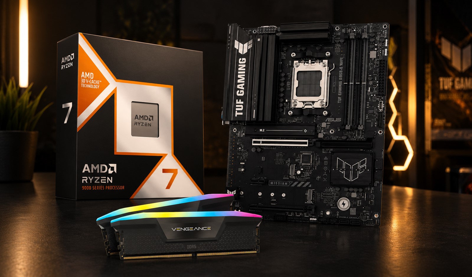
- 3D stacking: Rather than just shrinking transistors laterally, the industry is stacking logic, memory, and other components vertically. AMD's 3D V-Cache and TSMC's SoIC technology add computational resources without shrinking the base transistors.
- Chiplet architecture: Disaggregating chips into smaller, modular chiplets improves effective yield and allows mixing process nodes, achieving better overall value than pushing everything to the leading edge.
- Advanced packaging: Technologies like CoWoS, Foveros, and hybrid bonding enable tighter integration of diverse components, effectively increasing system-level transistor density.
- Specialized architectures: Rather than relying on general-purpose transistor improvements, the industry increasingly uses specialized hardware (GPU tensor cores, AI accelerators, neural processing units) to achieve dramatic speedups for specific workloads.
- Software and algorithm improvements: Advances in compilers, AI model architectures, and software optimization often deliver performance improvements that outpace hardware gains.
The Technologies Enabling Continued Scaling
Gate-All-Around Transistors
The FinFET transistor architecture, introduced at the 22nm node and used through 3nm, is reaching its scaling limits. Gate-all-around (GAA) transistors, in which the gate electrode wraps completely around the channel, provide better electrostatic control and enable continued scaling to 2nm and beyond. Samsung introduced GAA at its 3nm node, and TSMC and Intel are implementing it at their respective 2nm/18A nodes.
GAA comes in two main forms: nanosheets and nanowires. Nanosheets, which use wider channels stacked vertically, are preferred for their balance of drive current and manufacturability. Current designs stack three or four nanosheets, and future nodes may increase the stack height or transition to complementary FET (CFET) architectures that stack p-type and n-type transistors vertically on top of each other, essentially doubling density without shrinking lateral dimensions.
Backside Power Delivery
Conventional chips deliver power through the same wiring layers that carry signals, creating competition for routing space. Backside power delivery moves the power supply network to the back of the wafer, freeing the front-side wiring for signals. Intel's PowerVia technology is the first implementation of backside power delivery in a production process (Intel 18A), and TSMC is developing a similar capability for its A14 (1.4nm) node.
Backside power delivery can improve logic density by 10-15% and reduce power delivery resistance, enabling higher clock speeds and lower power consumption. It represents one of the most significant architectural changes in chip manufacturing in decades.
New Materials and Devices
Looking further ahead, the industry is exploring materials beyond silicon that could enable continued scaling. Carbon nanotube transistors have demonstrated excellent properties in research settings but face manufacturing challenges at scale. Two-dimensional materials like molybdenum disulfide could enable extremely thin channels with better electrostatic control than silicon at the smallest dimensions.
At the device level, negative capacitance transistors, tunnel FETs, and spintronic devices represent fundamentally different approaches to computing that could extend the performance trajectory beyond what silicon-based transistors can achieve. However, these technologies are at least a decade from commercial viability.
Beyond Moore's Law
The semiconductor industry has implicitly accepted that the Moore's Law era of simply shrinking transistors is nearing its end. TSMC's roadmap extends to the A10 (1nm) node around 2030, but the physical limits of silicon-based transistors become increasingly constraining at those dimensions. Gate lengths approaching 5 nanometers mean the channel is only about 10-15 atoms across, and quantum tunneling effects make further miniaturization extremely difficult.
The industry is already shifting its narrative from Moore's Law to what some call More-than-Moore, emphasizing the combination of transistor improvements, 3D integration, advanced packaging, specialized architectures, and software co-design that collectively continue to deliver exponential improvements in computing capability. This approach is messier and less elegant than simply shrinking transistors, but it is effective, and it will sustain the computing industry's growth trajectory for at least another decade.
Gordon Moore himself, who passed away in March 2023, acknowledged that his observation was never meant to be a permanent physical law. But the principle it embodied, that engineering ingenuity can deliver sustained exponential improvement, has proven remarkably durable. The form of that improvement is changing, but the pace of innovation in semiconductor technology shows no signs of slowing down.