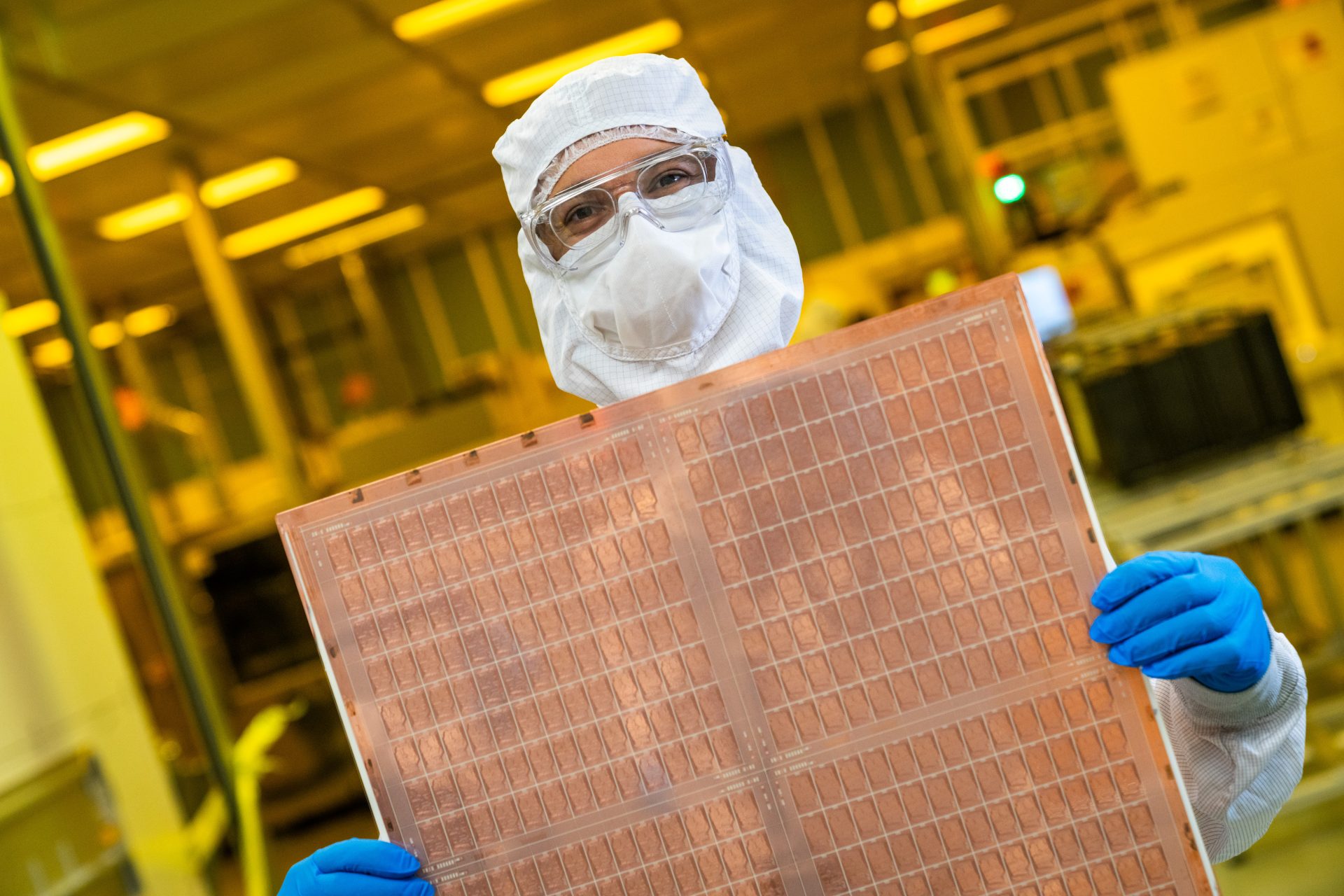
Look, another shiny new semiconductor material. This time it’s glass substrates, and wouldn’t you know it, Intel Foundry is leading the race to mass-produce them at their Rio Rancho facility. Yes, the same Rio Rancho that’s been around since the Reagan administration and was once the undisputed king of chipmaking. Now it’s being rebranded as the ‘Crown Jewel’ for… wait for it… glass. Because apparently, organic substrates are getting cramped and cranky thanks to the AI feeding frenzy. Ajinomoto, a big player in this game, is already jacking up prices, so naturally, everyone’s scrambling for a life raft. Enter glass substrates, which Intel assures us will magically solve warpage issues and pack in more density than a sardine can at a metal concert. They even showed off a shiny prototype with EMIB advanced packaging, and suddenly, Apple and Tesla are sniffing around like alley cats at a fish market. It’s all very convenient, isn’t it?
Now, I’ve seen these ‘next big things’ come and go for two decades. Remember graphene? Or those magical quantum dots that were supposed to revolutionize everything? They usually follow a predictable pattern: a lot of breathless PR, a few carefully curated demos, and then a slow fade into obscurity unless there’s a truly massive profit motive attached. Intel’s PR machine is in overdrive, naturally, painting Rio Rancho as the savior of semiconductor packaging. They’re talking about ‘unprecedented densities’ and ‘superior interconnects,’ all while conveniently forgetting that this stuff is still mostly on pilot lines or in the R&D phase.
Who’s Actually Making Money Here? (Besides Intel, Maybe)
The real question, as always, is who stands to gain the most financially? Intel Foundry, obviously. They’re betting big that this advanced packaging play will finally propel them past their foundry rivals. And if Apple, Tesla, Google, Microsoft, and NVIDIA – all names being bandied about as potential partners – actually sign on the dotted line for substantial orders, then yeah, Rio Rancho could indeed become a very important place. But let’s not forget that these companies are notoriously fickle. They’ll flirt with anyone offering a slightly better deal or a perceived technological edge, only to jump ship if something shinier floats by. So, while Amkor’s lead engineer is bravely predicting commercialization in three years, I’ll believe it when I see the invoices.
The buzz around silicon photonics, also supposedly happening at Rio Rancho, adds another layer to the narrative. Faster data center interconnects, less reliance on copper, lower power consumption – it all sounds fantastic. But again, we’re talking about tech that’s still largely in its infancy. Prototypes were showcased, aiming for a 2030 rollout. That’s a long way off, folks. Plenty of time for the market to shift, for competitors to emerge, or for the whole thing to be deemed too expensive or too difficult to scale.
Intel’s bets in its Foundry business seem to be paying off really well. There was a time when reports suggested that Intel would spin off its Foundry business, but today, Intel Foundry is set to become its biggest revenue generator if everything sails smoothly.
This quote from the original piece is telling. ‘If everything sails smoothly.’ That’s a big ‘if’ in this industry. Intel has a history of overpromising and underdelivering on manufacturing prowess. Remember the 10nm debacle? This feels like another high-stakes gamble, where the payoff is immense, but the risks are equally colossal. Rio Rancho’s history as a manufacturing powerhouse is real, but history doesn’t automatically translate to future success. It’s a factory, a really big, expensive factory, and its future success hinges on whether these glass substrates, and the silicon photonics they’re paired with, can actually deliver on the lofty promises and become economically viable on a massive scale.
Why All the Fuss Over Glass Substrates?
Intel claims these glass substrates are the answer to the industry’s packaging woes, particularly the strain caused by the AI boom. Traditional organic substrates are hitting their limits – they’re prone to warping under the intense heat and pressure of high-performance chips, and they simply can’t accommodate the sheer density of connections needed for modern AI accelerators. Glass, being more rigid and thermally stable, offers a potential solution. It allows for finer interconnects, meaning more data can be shuttled around the chip more efficiently. Plus, with global supply chains constantly on edge, having a domestic, high-volume source for these critical components would be a massive win for Intel and its partners. It’s a play for strategic advantage as much as it is for technological superiority.
Will This Replace My Job?
For the average consumer, this is unlikely to have a direct, immediate impact on your daily life. The advancements in glass substrates and silicon photonics are primarily aimed at high-performance computing, data centers, and potentially advanced AI chips. Think servers, supercomputers, and the next generation of specialized AI hardware. While these technologies eventually trickle down into consumer products, it’s usually a long process. For individuals working in the semiconductor manufacturing or design space, especially those involved in advanced packaging, this represents a significant shift. It could create new job opportunities in specialized areas, but also potentially make older skillsets less relevant. The industry is always evolving, and staying adaptable is key.
Is Intel’s Glass Substrate Tech Really New?
Glass has been explored as a substrate material for a long time, but mass-producing it reliably and economically for semiconductor manufacturing has been the major hurdle. Intel’s claim to fame here is developing the processes and infrastructure to achieve volume production, specifically at its Rio Rancho facility. They’re integrating it with other advanced packaging technologies like EMIB and potentially co-packaged optics. So, while the concept of glass substrates isn’t entirely novel, Intel’s push for mass production and its integration into their foundry services could be a significant differentiator if they pull it off successfully.