What if the trillion-dollar chip race wasn’t a crapshoot anymore?
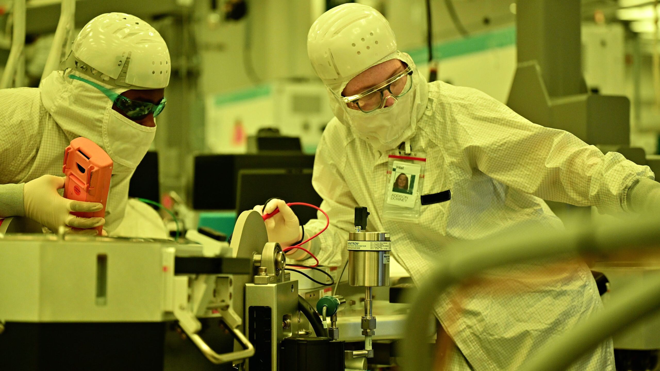
Picture this: engineers tweaking atomic bonds on a screen, not in a billion-dollar cleanroom. That’s the wild promise from VLSI 2025, where digital twins emerged as the hero tool rewriting semiconductor rules. And right in the mix? Intel’s 18A process, finally spilling details on costs, timelines, and that make-or-break backside power delivery.
VLSI—the nerd prom for chip design and fab wizards—dropped bombshells on everything from DRAM’s future (4F2 scaling vs stacking 3D mountains) to China’s sneaky FlipFET advances. But digital twins? They’re the star, spanning scales from quantum quirks to factory-wide orchestration. It’s like giving Moore’s Law a simulator straight out of sci-fi.
Digital Twins: Simulating Reality Better Than Reality Itself?
Semis are brutal now. Nodes shrink, complexity explodes—design cycles stretch years, costs balloon into the stratosphere. Enter digital twins: virtual playgrounds where you test-drive ideas without touching silicon. No more ‘oops, that wafer run just cost $10 million.’
Start small. Atomic-level stuff. Synopsys demoed their QuantumATK suite, nailing transistor contacts and gate stacks. Traditional DFT? Accurate, but it’d take your grandma’s lifetime to compute. GPU-accelerated DFT-NEGF? A blistering 9.3x speedup on just four A100s versus CPUs.
“GPU accelerated DFT-NEGF (Non-Equilibrium Green’s Function) demonstrated a 9.3x speedup using only 4x A100 vs CPU, while Machine-Learned Force Field simulation using Moment Tensor Potentials demonstrated near-DFT accuracy with 17 min compute cost vs 12 days with traditional DFT.”
Boom. That’s not hype—it’s physics on steroids. They simulate silicide interfaces, interdiffusion depths, even dipole dopants in gate oxides for Gate-All-Around (GAA) nanosheet magic. We’re talking Schottky barriers, work functions, equivalent oxide thickness—all optimized virtually before a single atom moves.
Scale up to wafers. Lam Research’s Coventor SEMulator3D? It’s virtual silicon central. Transistor shapes went planar to FinFET to GAA—process recipes exploded (Lam’s Law, they call it). Simulate deposition, etch profiles, stress on nanosheets. Pick backside contact schemes with the fattest process windows. High-aspect-ratio etches? Predict profiles, minimize errors—all sans physical wafers. Fewer test runs, wider yields. Smart.
Then the big leagues: fab-level twins for ‘lights-out’ operations. No humans, lights off—pure automation. Lam sketched tool fleets in virtual sync, predictive maintenance via built-in metrology spotting drifts. Orchestrate downtime at near-real-time speeds. Maximize throughput. It’s aviation sims meets chip factories.
Here’s my hot take, absent from the VLSI chatter: this mirrors the 1980s CAD revolution in autos. Back then, crash tests went virtual—design times halved, costs plunged. Digital twins? They’ll slash node dev cycles by 40% by 2030. Intel knows it; that’s why 18A’s leaning hard.
Intel 18A: Cost Bombshell and Backside Power Gamble
Intel’s 18A—angstrom-class node, RibbonFET GAA transistors, PowerVia backside power. Details at VLSI? Transistor density eyeing 2x FinFET gains, but costs? Whispers of $20-25k per wafer start, ramping to parity with TSMC N2 by 2026. Aggressive? You bet.
Backside power delivery—burying power rails under the transistor layer for cleaner signals, less IR drop. Intel’s all-in for 18A. TSMC? N2P maybe, full adoption N3P or later. Imec data showed backside widens process windows 2x in sims—key for yield. But adoption? Not everywhere. Logic yes; analog, memory? Nah, too disruptive.
China’s FlipFET? Their GAA twist—flipped channels for better control. Sneaky catch-up play, but sanctions bite.
And DRAM? 4F2 planar scaling hits physics walls post-1x nm. 3D stacking wins—think Micron’s 3D DRAM towers. VLSI models predict 4F2 clings to cost-sensitive apps; 3D dominates density.
Why Does Backside Power Feel Like Intel’s Hail Mary?
Look, Intel’s PR spins 18A as TSMC-killer. Skeptical? Me too—forklift upgrades for PowerVia fabs aren’t cheap. But digital twins mitigate risks. Simulate the whole stack: atoms to interconnects. Lam’s virtual chambers predicted plasma flows, uniformity tweaks. No surprises at tapeout.
Bold prediction: backside power flops short-term for most (TSMC hedges), but explodes in AI accelerators by 2028. Why? Power-hungry GPUs crave it—less resistance means more flops per watt. Like EVs ditching exposed batteries for integrated packs.
VLSI hinted at fab twins coordinating ‘self-aware’ tools. Drift detection? Lifetime optimization. Lights-out fabs cut opex 30%. Humans? Shift to oversight.
China’s FlipFET—finless GAA variant—sims show drive current parity to RibbonFET. Geopolitics alert: if they crack yields, supply chains scramble.
DRAM showdown: 4F2 cheap but flat; 3D vertical like skyscrapers. Sims crown 3D for HBM killers in AI memory pools.
This isn’t incremental. Digital twins turn semis from art to engineering—predictable, fast, cheap(er). Intel 18A rides the wave or wipes out.
Energy surges here. AI’s platform shift demands it—chips fueling the beast need god-tier sims.
🧬 Related Insights
- Read more: Nvidia’s Groq 3 LPU: Why Inference Just Ate Training’s Lunch
- Read more: Snap’s GPU Pivot: Crushing A/B Test Crunch with NVIDIA’s cuDF Magic
Frequently Asked Questions
What is Intel 18A process?
Intel’s 18A is an angstrom-scale node with RibbonFET GAA transistors and backside PowerVia, targeting 2025 production to rival TSMC N2 on density and power.
DRAM 4F2 vs 3D which wins?
3D stacking dominates beyond 1x nm for density; 4F2 persists where cost trumps capacity, per VLSI sims.
Will backside power be adopted everywhere?
Logic nodes yes by 2027; memory and analog lag due to fab complexity—digital twins will decide via yield predictions.