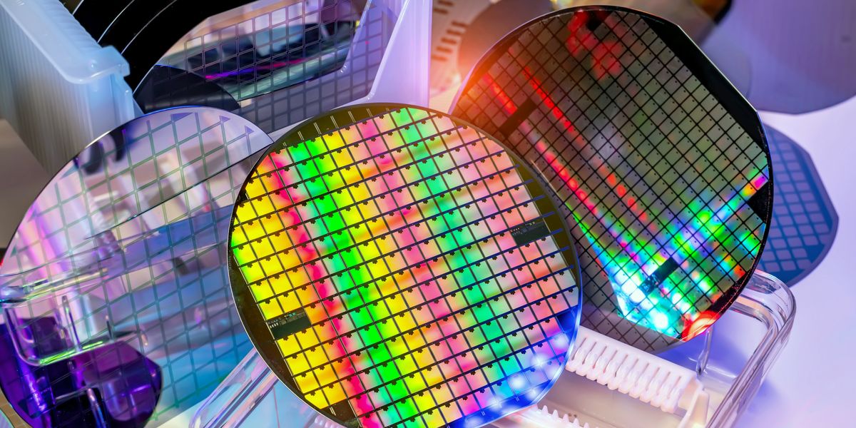
A single silicon wafer, pristine under the stark glare of a cleanroom, gleamed with the promise of a future not yet built.
The announcement from imec this week landed with a quiet thud, rather than the usual quantum computing fanfare. They’ve built the world’s first quantum dot qubit device using High-NA EUV lithography. On the surface, it sounds like just another entrant in the crowded quantum race. But dig a little deeper, past the qubit counts and coherence times, and you’ll find something far more profound: a potential solution to quantum computing’s existential manufacturing crisis.
Qubits, these ephemeral flickers of quantum information, hold the theoretical key to solving problems that would baffle even the most potent supercomputers. Yet, the chasm between theoretical possibility and practical, scalable machines remains vast. For years, the bottleneck wasn’t the physics—it was the sheer, agonizing difficulty of manufacturing these delicate devices with the precision required. Imec claims to have just plugged that hole, using the semiconductor industry’s absolute cutting edge to etch silicon quantum dot spin qubits with tolerances that, for the first time, speak the language of industrial chip production.
Manufacturing, not physics, is now quantum computing’s major bottleneck
It’s a fascinating pivot. The headlines typically shout about new qubit architectures or ever-longer coherence times. But the real slog, the unglamorous grind, has been scaling. Companies like IBM, Google, IonQ, and others have demonstrated working prototypes across a spectrum of technologies—superconducting circuits, trapped ions, photonics. The shared, unstated reality is that scaling these systems to the millions of reliable, interconnected qubits needed for fault-tolerant, commercially useful computation is a monumental engineering and manufacturing challenge. Industry roadmaps often punt that horizon to 2030 and beyond, a clear signal that the physics are mostly there; it’s the factory floor that’s lagging.
Imec’s approach, however, is built on an industry’s existing, deeply entrenched foundation: silicon. Their quantum dots are designed to use conventional CMOS semiconductor manufacturing infrastructure. Think of it as trying to build a spaceship using parts and techniques already perfected for building millions of cars. It’s an attempt to piggyback on the decades of R&D and the colossal manufacturing muscle of the established chip industry, rather than building an entirely new fabrication ecosystem from scratch.
The mechanics are elegant in their abstraction. Individual electrons are trapped within tiny silicon structures—the quantum dots. Their quantum spin state encodes information. Control gates, mere nanometers away, whisper instructions to these entangled electrons, orchestrating their interactions. The devil, as always, is in the details—specifically, the impossibly small gaps between these control electrodes. As these gaps shrink, the coupling strength between neighboring quantum dots increases exponentially, leading to greater controllability and fidelity. But achieving these gains requires patterning features at the 6-nanometer scale, reliably, across an entire wafer.
This is where High-NA EUV steps in. Imec reports fabricating functional qubit arrays with 6nm gaps using ASML’s latest High Numerical Aperture Extreme Ultraviolet lithography system. This isn’t just a tweak; it’s the next frontier in chip patterning, designed for the sub-2nm nodes that will power future processors and AI accelerators.
High-NA EUV: not yet standard, already essential
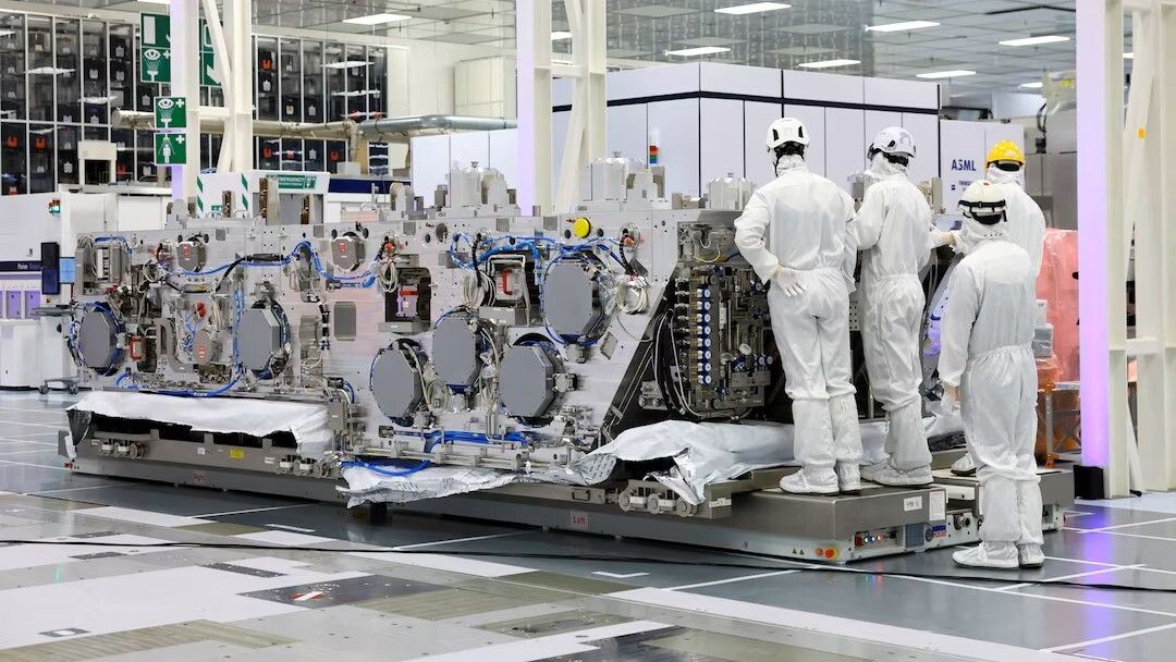
The machinery behind High-NA EUV is staggering. We’re talking about a 150-ton behemoth, the length of a double-decker bus, an optical system with mirrors twice as large and ten times heavier than conventional EUV, all polished to near-atomic perfection by ZEISS. It’s an engineering tour de force years in the making. And it’s just now beginning to enter commercial deployment within mainstream semiconductor foundries, primarily for the most advanced logic and memory chips.
“If that holds up, the implications for quantum scaling could be tremendous. It’s a significant step towards quantum computing, but we are still not quite there.”
This is the core of imec’s gamble, and its potential triumph. By demonstrating that High-NA EUV can reliably fabricate the extraordinarily precise structures required for silicon quantum dots, they’re effectively saying: the tools we use to build the world’s most advanced classical chips can also build advanced quantum chips. This isn’t just about improving qubit fabrication; it’s about pulling quantum computing onto the same manufacturing roadmap as the processors that are already turbocharging AI. It’s about compressing timelines, not by magic, but by shared infrastructure.
This has massive implications. If imec’s breakthrough proves out, it means quantum computers might not need entirely separate, incredibly expensive, and slow-to-develop manufacturing lines. They could, in theory, benefit from the same iterative improvements, the same economies of scale, and the same relentless drive for precision that has defined the semiconductor industry for half a century. It’s a move from the laboratory bench to the industrial assembly line, a transition that has always been the true test for any nascent technology aiming for broad impact.
There’s a subtle critique here, too, embedded in the technical achievement. The PR often buzzes about quantum supremacy or the potential to solve specific grand challenges. But the real breakthrough, the one that hints at commercialization, is often hidden in the dull, vital details of how you actually make the thing. Imec’s work is a potent reminder that the most significant advances can sometimes be less about the fundamental discovery and more about the painstaking engineering required to bring it to scale.
My unique insight? This imec announcement isn’t just about building better qubits; it’s about synchronizing the clock speeds of quantum hardware development with the relentlessly accelerating cadence of AI hardware manufacturing. For years, quantum has been on its own slow, deliberate timeline. Now, it’s potentially hitching a ride on the express train of next-gen processor fabrication. This isn’t just a step forward; it’s a potential phase shift in how we think about quantum hardware development timelines.
The path to fault-tolerant quantum computing is still long, littered with engineering hurdles and scientific unknowns. But by bridging the gap between exotic quantum hardware and bleeding-edge silicon manufacturing, imec has undeniably brought that future into sharper focus, and perhaps, a lot closer than we might have thought.
🧬 Related Insights
- Read more: Truck-Sized AI Data Centers: GPUs Delivered in Months, Not Years
- Read more: CAST’s xSPI IP Core: Real-World Memory Control for Safety-Critical Systems
Frequently Asked Questions
What does High-NA EUV lithography do? High-NA EUV lithography is an advanced chip manufacturing technique that uses a higher numerical aperture in its optical system to pattern extremely small and precise features onto silicon wafers, enabling the production of next-generation processors.
Will this make quantum computers available sooner? Imec’s breakthrough in using High-NA EUV for qubit fabrication suggests that quantum computers could potentially use the same advanced manufacturing infrastructure as classical processors, which might accelerate their development and scalability.