Modern chips contain billions of transistors arranged in intricate patterns on a piece of silicon smaller than a fingernail. No human could design such complexity manually. Instead, chip designers rely on a category of software called Electronic Design Automation, or EDA, which automates the process of designing, simulating, verifying, and preparing semiconductor chips for manufacturing. The EDA industry is a $15 billion market dominated by three companies, and it represents one of the most critical chokepoints in the global semiconductor supply chain.
What EDA Tools Do
Chip design is an enormously complex process that transforms a high-level description of a chip's intended behavior into a detailed physical layout specifying the exact position of every transistor, wire, and contact on the silicon die. EDA tools manage this transformation through a series of stages, each requiring specialized algorithms and immense computational resources.
The process begins with specification and architecture definition, where designers determine what the chip should do. It then moves through register-transfer level (RTL) design, where the chip's logic is described in hardware description languages like Verilog or SystemVerilog. From there, the design flows through logic synthesis, which converts the RTL description into a network of logic gates. Place and route tools then determine where each gate should be positioned on the chip and how they should be connected with metal wires. Finally, physical verification tools check that the layout meets the foundry's manufacturing rules.
At each stage, verification tools ensure the design is correct. Simulation checks that the chip behaves as intended. Formal verification mathematically proves that certain properties hold. Timing analysis confirms that signals arrive at their destinations within required timeframes. Power analysis estimates the chip's energy consumption. These verification steps consume the majority of a chip's development time and compute resources.
The Big Three: Synopsys, Cadence, and Siemens EDA
Three companies control approximately 80 percent of the EDA market: Synopsys, Cadence Design Systems, and Siemens EDA (formerly Mentor Graphics, acquired by Siemens in 2017). Each offers a comprehensive suite of tools covering the full chip design flow, though each has historical strengths in specific areas.
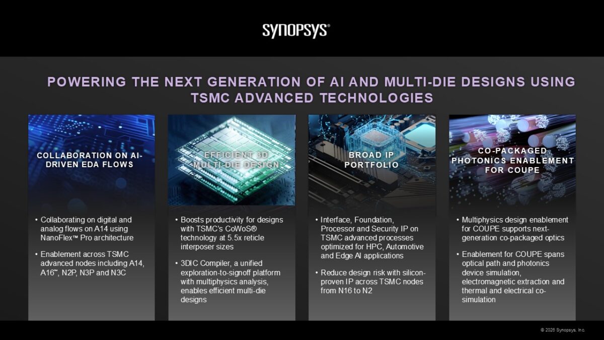
Synopsys
Synopsys is the largest EDA vendor by revenue, generating over $6 billion annually. The company's Design Compiler remains the industry standard for logic synthesis, the critical step that converts RTL code into gate-level netlets. Synopsys also leads in static timing analysis with PrimeTime, formal verification with Formality, and design-for-test with its DFT Compiler. The company's Fusion Compiler offers an integrated synthesis and place-and-route flow that aims to optimize results across traditionally separate stages.
Cadence Design Systems
Cadence matches Synopsys in market capitalization and revenue, with particular strength in custom and analog design. The Cadence Virtuoso platform is the dominant tool for designing analog circuits, mixed-signal blocks, and memory cells, areas where automated digital flows cannot replace human expertise. Cadence's Innovus place-and-route tool is widely used for advanced node digital designs. The company's Xcelium simulator and JasperGold formal verification tools are also industry standards.
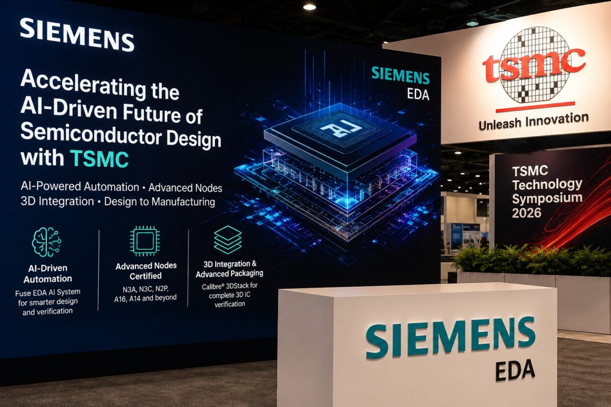
Siemens EDA
Siemens EDA holds a smaller market share than Synopsys or Cadence but leads in specific areas. Calibre, its physical verification tool, is the industry standard for design rule checking (DRC) and layout versus schematic (LVS) verification at leading-edge nodes. Virtually every chip taped out at TSMC, Samsung, or Intel goes through Calibre verification before manufacturing. Siemens also offers HyperLynx for PCB-level signal integrity analysis and Questa for simulation and verification.
The Design Flow in Detail
A typical digital chip design flow involves dozens of EDA tools used in sequence and in parallel. Understanding this flow reveals why EDA is so essential and why switching between tool vendors is so difficult.
RTL Design and Simulation: Engineers write the chip's logic in SystemVerilog, describing registers, arithmetic units, controllers, and interfaces. Simulation tools like Synopsys VCS or Cadence Xcelium execute this code against test scenarios to verify correct behavior. A complex chip might require millions of simulation cycles consuming thousands of CPU hours.
Logic Synthesis: Tools like Synopsys Design Compiler translate the RTL description into a netlist of standard cells, pre-designed logic gates from a library provided by the foundry. The synthesis tool optimizes for speed, area, and power consumption based on designer-specified constraints.
Place and Route: The synthesized netlist must be physically implemented on silicon. Place-and-route tools like Cadence Innovus or Synopsys IC Compiler II determine where each standard cell should be positioned and how metal wires should connect them. This step is extraordinarily complex at advanced nodes, where a chip might contain billions of cells and hundreds of kilometers of interconnect wires spread across more than 15 metal layers.
Physical Verification: Before sending the design to the foundry, physical verification tools check every aspect of the layout. DRC ensures all features meet the foundry's minimum spacing and width requirements. LVS confirms the physical layout matches the intended circuit schematic. Extraction tools calculate the parasitic capacitance and resistance of every wire, which is fed back into timing analysis to verify that the chip will operate at its target frequency.
- Simulation time for a complex SoC: weeks to months of continuous computation
- Place and route iterations: typically 5-20 iterations to meet all constraints
- Physical verification rules at 3nm: tens of thousands of individual checks
- Total EDA license cost for a large chip team: $50-200 million annually
Why EDA Is a Strategic Chokepoint
The concentration of EDA technology in three American companies has significant geopolitical implications. U.S. export controls imposed in 2022 restrict the sale of advanced EDA tools to China, specifically targeting tools needed for chip design below 14nm. Without access to these tools, Chinese chip designers cannot create leading-edge processors regardless of whether they have access to advanced manufacturing equipment.
This chokepoint exists because EDA tools represent decades of accumulated algorithmic innovation that is extremely difficult to replicate. The place-and-route algorithms alone embody solutions to NP-hard optimization problems that have been refined over 30 years. China has invested heavily in domestic EDA development, with companies like Empyrean and Primarius receiving government support. However, these tools remain generations behind their Western counterparts at advanced nodes, and closing this gap will require years of sustained effort.
The Future: AI in EDA
Artificial intelligence is beginning to transform EDA itself. Google's 2021 publication on using reinforcement learning for chip floor planning generated significant attention and controversy, but the broader trend is unmistakable. All three major EDA vendors are incorporating machine learning into their tools to predict design outcomes, optimize placement decisions, and reduce the number of iterations needed to close timing.
Synopsys's DSO.ai (Design Space Optimization AI) uses reinforcement learning to explore the vast parameter space of synthesis and place-and-route tools, automatically finding configurations that produce better results than human engineers can achieve through manual tuning. Cadence's Cerebrus applies similar techniques to its tool suite. These AI-assisted flows can reduce design closure time by 30 to 50 percent in some cases.
EDA tools are the invisible foundation upon which the entire semiconductor industry rests. Without them, the chips powering everything from smartphones to data centers to automobiles simply could not be designed. The EDA industry's small size relative to the semiconductor market belies its outsized importance as both a technical enabler and a strategic asset.