The whispers had grown to a roar. For months, the tech world’s collective gaze was fixed squarely on the silicon brain—the AI accelerators, the GPUs that were supposedly going to buckle under the sheer weight of the AI revolution. We were all bracing for a compute crunch, a digital dam about to burst. And then, like a sudden shift in the tectonic plates of innovation, the conversation pivoted. The real bottleneck, it turns out, isn’t the thinking; it’s the talking.
Look, if you’re building a city, you can have the most brilliant architects and engineers designing skyscrapers, but if you don’t have enough roads, enough power lines, enough sewage systems to connect them all, your city grinds to a halt. That’s where AI is heading. The raw processing power of these massive AI clusters is becoming less important than the speed, efficiency, and sheer volume of data that can be ferried between them. And copper cables? They’re about as effective as a single-lane dirt track in this new metropolis.
This is where Scintil Photonics is making its move, and frankly, it’s a move that feels less like an iteration and more like a fundamental platform shift. They’re not just building faster chips; they’re building a fundamentally new way for chips to talk to each other, and they’re doing it with light. They call their approach SHIP™ – Scintil Heterogeneous Integrated Photonics. It sounds like something out of a sci-fi novel, but the implications are decidedly grounded in the here and now.
Think back to the dawn of the integrated circuit. Before, you had clunky, discrete components soldered onto circuit boards. Then came the silicon wafer, and suddenly, millions of transistors could live together on a single chip. Photonics, the science of light, is essentially going through that same seismic shift, and Scintil is planting its flag right at the epicenter. Their SHIP process allows them to bond III-V gain material—the stuff that makes lasers and other active photonic components sing—directly onto a silicon photonics wafer. The result? Lasers, modulators, detectors, all on the same tiny piece of silicon, all flowing through the same high-volume foundry processes that churn out the transceivers we use today.
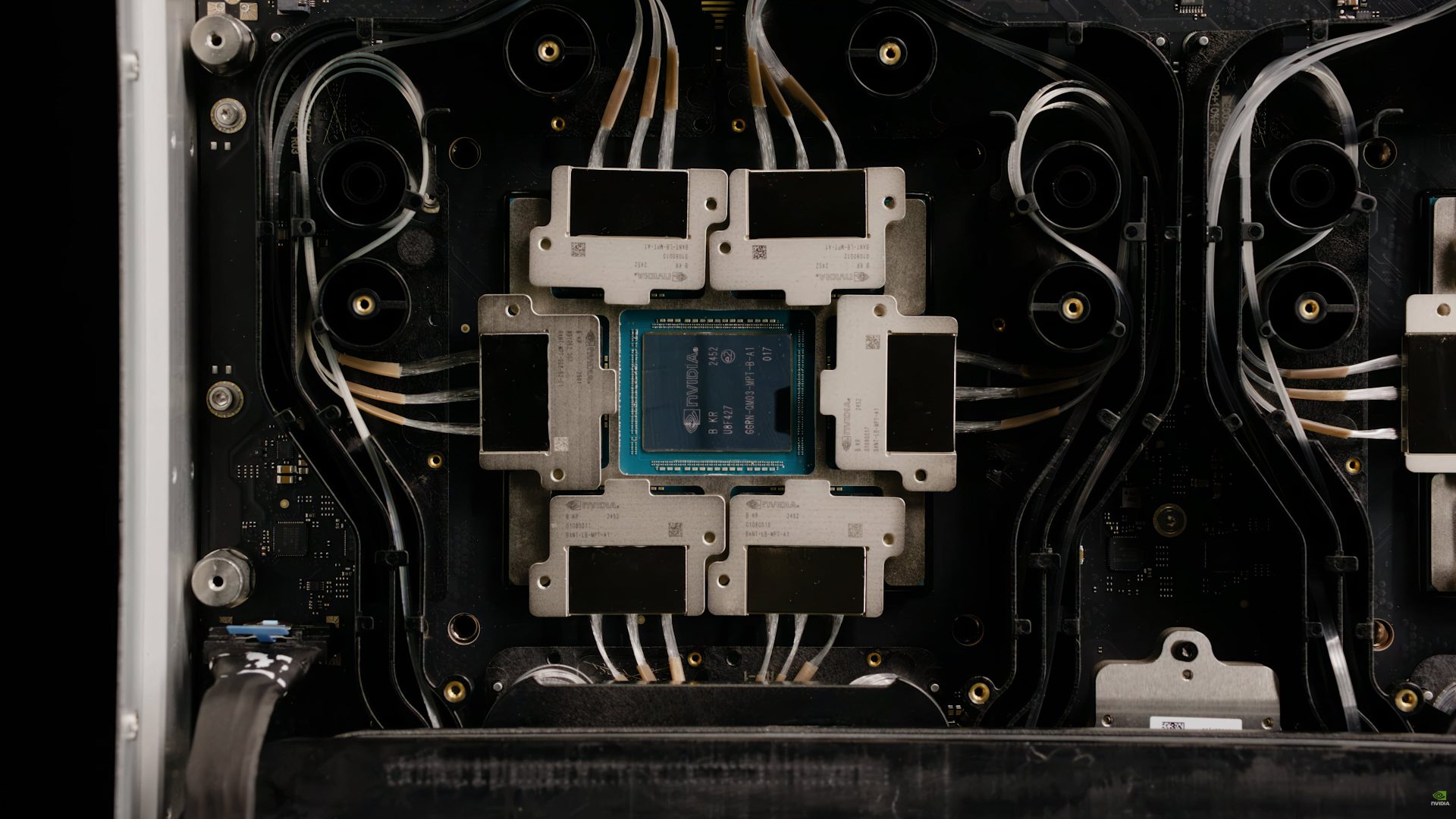
Their flagship product, LEAF Light™, is a single-chip DWDM (Dense Wavelength Division Multiplexing) laser source designed explicitly for these gargantuan AI networks. And get this: NVIDIA, the undisputed king of AI accelerators, is a backer. That’s not just a vote of confidence; it’s a full-blown endorsement from the guys who understand AI infrastructure better than almost anyone on the planet.
Why Is the Network Suddenly the Star of the Show?
Matt Crowley, Scintil’s CEO, puts it plainly: “The hardest problem in AI infrastructure right now is not compute. It is the network between compute elements.” Imagine thousands of AI processors, all working in concert. If the data can’t flow fast enough between them, if the latency is too high, or if the energy consumed just to move that data is astronomical, then all that fancy compute power becomes… well, useless. Copper has hit its wall. It’s like trying to quench a wildfire with a teacup.
So, what’s the next step? Dense Wavelength Division Multiplexing (DWDM) on co-packaged optics (CPO) for what Scintil calls “scale-up” networks. This is where you pack multiple wavelengths of light onto a single fiber, essentially creating multiple superhighways within one physical cable. This needs a multi-wavelength light source that’s not just precise but can be manufactured at hyperscale volumes. That has been the missing piece. Until now, perhaps.
Scintil’s differentiator is stark. They’re not fiddling with discrete laser arrays that require endless assembly steps for each additional wavelength. They’re not relying on exotic mode-locked lasers that are notoriously difficult to manufacture reliably at scale. Their heterogeneous integration approach, their SHIP process, means that adding another wavelength is akin to adding another transistor to a chip. The cost curve, for the first time, looks like a semiconductor learning curve, not a plodding assembly line.
“By bonding III-V gain material directly onto a silicon photonic wafer in a foundry process, we put lasers, modulators, detectors, and passive photonics on the same die, in the same flow, on the same lines that already produce tens of millions of optical transceivers a year.”
This isn’t just about making things slightly better; it’s about re-architecting the very foundations of how AI systems communicate. Customers aren’t just looking for a solution for today; they’re demanding a roadmap. They need to know that the optical layer they invest in today will scale with their ambitions for multi-rack, petascale AI clusters without requiring a complete overhaul every two years. This demand for a clear pathway to future performance is where many in the industry falter, but it’s precisely the question Scintil believes its foundry-resident process flow can answer.
The narrative here is potent: AI’s insatiable appetite for data is finally forcing a rethink of the plumbing. While compute gets the headlines, the unsung heroes of the data center are the engineers figuring out how to keep the information flowing. Scintil Photonics isn’t just participating in this shift; they’re actively trying to define its architecture. It’s an ambitious play, but one that, if successful, could redefine the very limits of what AI can achieve.
One fascinating angle that’s often overlooked in the rush for faster components is the sheer inertia of infrastructure. Fiber optic cabling, once laid, is incredibly expensive to rip out and replace. By enabling more wavelengths on existing fibers through DWDM integrated photonics, Scintil’s approach offers a way to drastically increase bandwidth without a corresponding explosion in cabling costs. It’s a brilliant economic lever, effectively allowing AI networks to scale up their capacity without scaling out their physical footprint in a prohibitive way. This isn’t just about the next generation of AI; it’s about making the entire ecosystem sustainable at scale.
🧬 Related Insights
- Read more: NVIDIA CloudXR 6.0: XR Streaming’s WiFi Savior or Bandwidth Bust?
- Read more: India’s 37 Supercomputers: Impressive Fleet, But Chips Still from Abroad
Frequently Asked Questions
What is Scintil Photonics’ SHIP technology?
SHIP (Scintil Heterogeneous Integrated Photonics) is Scintil’s proprietary process for integrating III-V gain materials directly onto silicon photonic wafers. This allows for the creation of dense, multi-functional photonic integrated circuits, including lasers, modulators, and detectors, on a single chip using high-volume foundry manufacturing.
Will this technology replace current AI network infrastructure?
Scintil’s technology is designed to address the limitations of current copper-based networks and to enable the next generation of AI scale-up networks using DWDM co-packaged optics. It represents a significant upgrade and architectural shift rather than a direct replacement of all existing infrastructure, focusing on high-performance AI clusters.
How does this compare to other approaches to DWDM light sources?
Scintil differentiates itself through heterogeneous integration at the wafer level, which offers a semiconductor-like cost scaling for adding more wavelengths, unlike discrete laser arrays or mode-locked lasers. This approach aims for higher integration, lower cost per wavelength, and manufacturability at hyperscale volumes.