Look, the numbers don’t lie. A 72.1% enhancement in thermal conductivity isn’t just an incremental bump; it’s a significant leap forward, especially when you’re talking about the scorching environment inside advanced semiconductor packaging. Georgia Institute of Technology and National Cheng Kung University have dropped a paper detailing how ultralong Al2O3 nanowires can tackle the ever-growing heat flux that threatens to bottleneck the performance of our latest 2.5D/3D chip designs. This isn’t just about making chips run a little cooler; it’s about ensuring they can reach their full potential without melting into a silicon puddle.
The Heat Is On
We’ve all seen the specs on the newest CPUs and GPUs. More cores, higher clock speeds, denser integration – and with all that power comes a tsunami of heat. For years, thermal interface materials (TIMs), those gooey or pad-like substances between the chip and its cooler, have been the unsung heroes (or sometimes, villains) of heat dissipation. Traditional epoxy-based TIMs are workhorses; they stick well, they’re easy to process, but their inherent thermal conductivity? Frankly, it’s lackluster. You need a boatload of conventional ceramic fillers to get them to behave, and that just makes them harder to work with, compromising the very processability they’re supposed to offer.
Enter the Nanowire Army
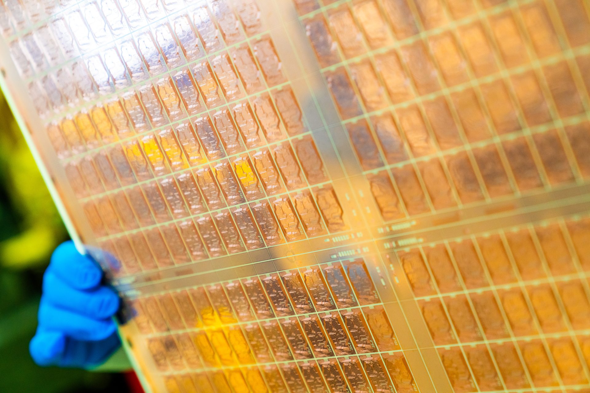
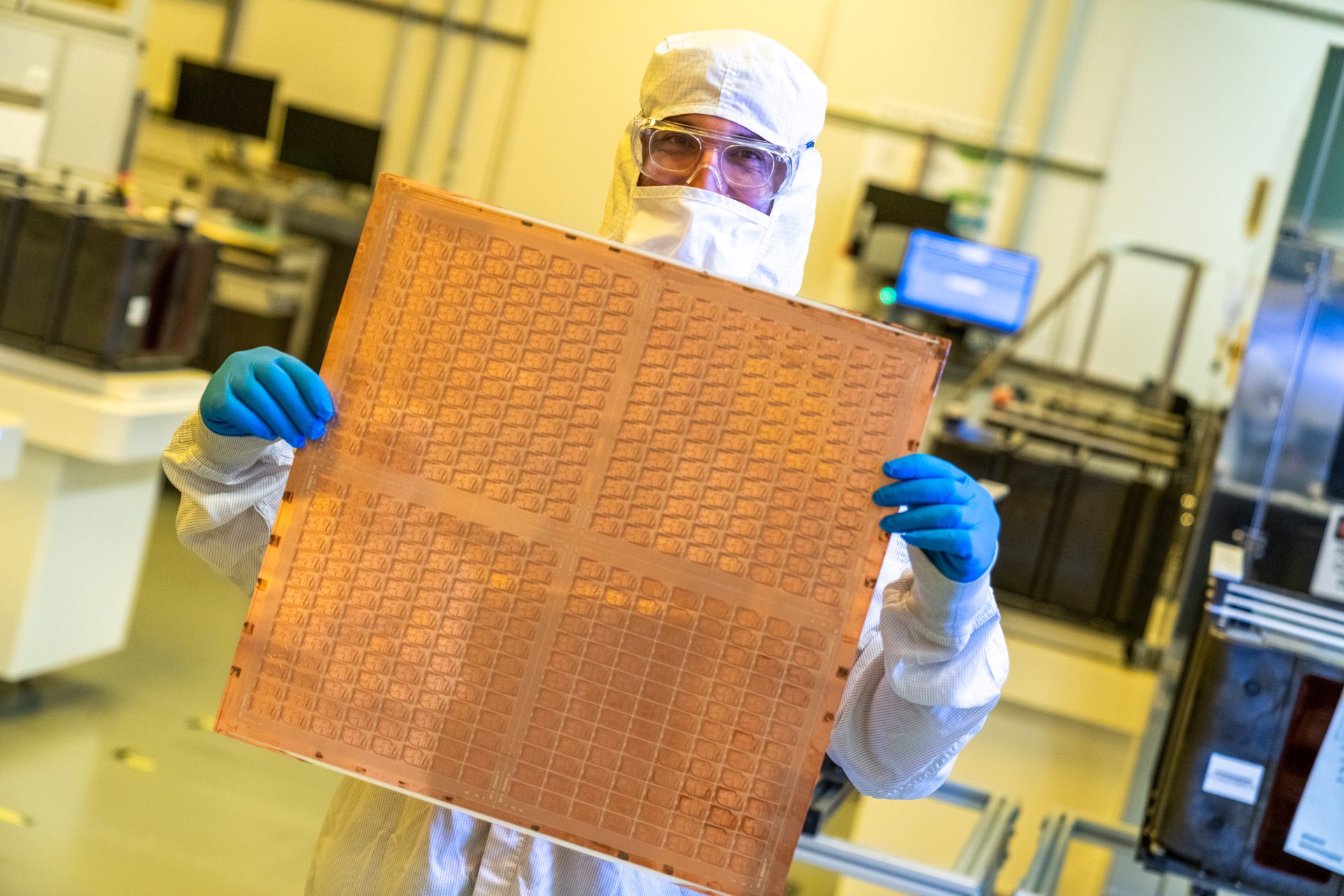
This is where the Georgia Tech team’s work shines. They’ve engineered ultralong alumina nanowires (ULANWs) that are absurdly thin – nanoscale diameters of 100–1000 nm – but astonishingly long, stretching to millimeter-scale. We’re talking an aspect ratio of around 1000, which is key. These aren’t your grandma’s chopped-up ceramic particles. Their elongated, spaghetti-like structure allows for much more efficient phonon transport, the mechanism by which heat moves through solids.
The researchers developed a scalable fabrication method for these ULANWs and then incorporated them into epoxy matrices. They didn’t just randomly dump them in, either. They explored two architectures: randomly dispersed networks and, more intriguingly, hierarchically structured vertically oriented sheets. This latter approach, where the nanowires are aligned in a specific direction, proved to be the real winner.
The Data Doesn’t Lie
The results are, frankly, staggering. At a filler loading of a mere 28 wt %, the vertically structured composite achieved an out-of-plane thermal conductivity of 0.78 W/(m K). Let’s break that down. That’s a 72.1% improvement over composites filled with traditional Al2O3 particles. And compared to the neat epoxy itself? A monumental 452.6% improvement. This means heat can escape the chip much, much faster, preventing those dreaded hotspots that can throttle performance and shorten a chip’s lifespan.
But it’s not just about conductivity. The ULANW network also does wonders for mechanical properties, suppressing thermal expansion – a huge deal in advanced packaging where mismatched expansion rates can cause serious reliability issues – and enhancing stiffness. Finite element simulations backed up the experimental findings, showing substantially reduced junction temperatures.
“The interconnected ULANW architecture reduces the interfacial thermal resistance and lowers the thermal percolation threshold.”
This quote, plucked right from the abstract, gets to the heart of it. It’s not just about stuffing more stuff into the epoxy; it’s about how that stuff is arranged and its inherent properties that allows heat to flow more freely across the interfaces.
A New Dawn for TIMs?
This research presents a compelling case for ULANWs as the next generation of TIMs. The ability to achieve such significant thermal enhancements at relatively low filler loadings is a massive win for processability. It suggests that we might finally be able to push the boundaries of semiconductor packaging without being perpetually held back by heat.
Of course, scaling up nanowire production to meet the demands of the semiconductor industry is always a challenge. And long-term reliability under extreme thermal cycling needs further investigation. But the fundamental science here is sound, and the potential impact is enormous.
What Does This Mean for Advanced Packaging?
This isn’t just a neat lab experiment; it has real-world implications. Advanced semiconductor packaging, think 2.5D and 3D stacking, is where the industry is heading to squeeze more performance out of silicon. These techniques allow for the integration of multiple chips or dies into a single package, leading to increased bandwidth and reduced latency. However, stacking chips on top of each other creates unprecedented thermal challenges. Heat generated by lower layers has to fight its way through multiple layers to escape, creating incredibly difficult thermal management scenarios.
The ULANW approach, particularly the vertically oriented structures, seems tailor-made for these stacked architectures. Imagine layers of nanowires acting like tiny, efficient heat pipes, guiding thermal energy directly out of the package. This could enable denser, more powerful stacked designs that were previously impossible due to thermal limitations.
The Bloomberg Take: Corporate Hype vs. Hard Data
Let’s be clear: there’s a lot of corporate noise and aspiration in the semiconductor industry. Companies talk about “breakthroughs” and “paradigm shifts” constantly. But then you get papers like this from Georgia Tech. It’s not a marketing press release; it’s a peer-reviewed technical paper backed by solid data and simulations. The researchers aren’t claiming to have solved all the world’s problems, but they’ve presented a very strong, data-driven argument for a superior material solution. They’re focused on the physics and the engineering, and that’s exactly what we need to see.
If this technology can be scaled economically, it could become a standard component in the thermal management toolkit for high-performance computing, AI accelerators, and next-generation mobile devices. It addresses a fundamental constraint that is becoming increasingly critical as chip complexity grows. It’s a tangible step forward, not just a fuzzy promise.
Why Does This Matter for Chip Designers?
For chip designers and architects, this development is a breath of fresh air. It means they have more headroom. They can push clock speeds higher, integrate more cores, and design more complex 3D architectures knowing that the thermal bottleneck might be significantly loosened. This isn’t about incremental improvements; it’s about unlocking new design possibilities. It means the dream of even more powerful, efficient, and compact electronic devices is a little closer to reality.
🧬 Related Insights
- Read more: RX 9070 XT at $720: AMD’s Price Slash Exposes NVIDIA’s Greed
- Read more: Daily Briefing: April 14, 2026
Frequently Asked Questions
What exactly are alumina nanowires? Alumina nanowires are incredibly thin, rod-like structures made of aluminum oxide, measured at the nanoscale (one-billionth of a meter) in diameter. They are extremely long relative to their width, giving them a high aspect ratio.
Will this replace all current thermal interface materials? It’s too early to say. While these ULANWs show significant promise, their cost-effectiveness, long-term durability under extreme conditions, and ease of integration into existing manufacturing processes will determine their widespread adoption. They are more likely to be used in high-performance applications initially.
How much does this technology cost to implement? The paper mentions a “scalable fabrication strategy,” which is positive. However, the actual manufacturing cost of producing these ULANWs in mass quantities and integrating them into TIMs is not detailed and will be a critical factor for commercial viability.