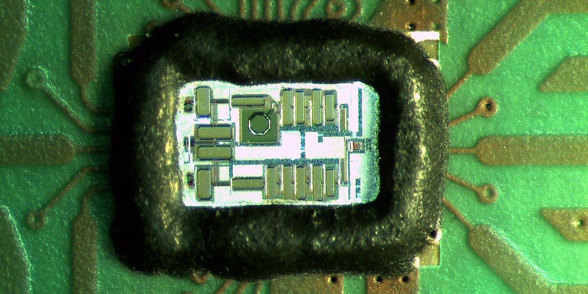
Everyone thought the UK semiconductor sector was busy staring into the abyss, lamenting a skills gap wider than the English Channel. We were told the old guard was retiring, and nobody was stepping up to learn the arcane arts of ASIC design. Then, bam. 120 students, ten universities, one afternoon. They didn’t just learn about chips; they designed them. Taped them out. That’s the part that actually makes you sit up and notice.
The Tiny Tapeout framework. Open-source. MPW schemes. Sounds like tech jargon designed to bore you into submission, right? Wrong. This is the secret sauce. It’s what made 120 students — many with zero prior experience — go from zero to silicon design, ready for fabrication, all before their pizza got cold. This isn’t just a single event; it’s apparently the biggest Tiny Tapeout workshop and mass tapeout cohort ever. Globally. Take that, industry experts who predicted doom.
A Generational Bridge, Built on Open Source?
The core problem: UK semiconductor sector bleeding talent, demand for chip designers soaring, and the old guard… well, they’re old. Add to that the usual suspects – restricted access to fancy EDA tools and fabrication facilities. Historically, this meant students were stuck drawing diagrams, not actually making things. It’s like teaching someone to cook by only showing them pictures of ingredients.
Tiny Tapeout flips the script. Open-source tools, combined with this multi-project wafer (MPW) magic, slash the cost. Suddenly, groups of students can get their hands on real silicon. It’s not just about theoretical knowledge anymore; it’s about messy, tangible, real-world application. The kind of experience that doesn’t fit neatly into a PowerPoint slide.
Dr. Mohammad Eissa, one of the masterminds behind this at the University of Sheffield, hits the nail on the head: “This initiative shows what is possible when academia, students and industry come together to remove barriers to chip design.” Exactly. No more excuses. Just students, tools, and the ambition to see their design etched in silicon.
“Giving students the opportunity to take a design all the way to silicon is incredibly powerful, but just as importantly, it helps raise awareness. Many students don’t initially consider semiconductors as a career path, and experiences like this can fundamentally change that.”
That’s the kicker, isn’t it? Most students don’t even think about chip design as a career. It’s seen as obscure, impenetrable. This kind of hands-on experience is the spark. It makes the abstract real. It ignites curiosity. And that’s something no amount of industry lobbying or government white papers can replicate.
Ian Lankshear from EnSilica, a sponsor, chimes in: “The UK semiconductor sector faces a well-documented skills shortage, and increasing the number of engineers with practical design experience is critical.” He’s not wrong. This isn’t a hobby for them; it’s about filling seats with competent, practically experienced engineers. This workshop provides that bridge between what’s taught in lectures and what’s actually done on the factory floor.
Is This the Silver Bullet?
Let’s not get carried away. 120 students is a start. A very good start, mind you, especially considering the scale and speed. But the UK needs thousands. This initiative is part of a broader push, working alongside groups like the UK Electronics Skills Foundation (UKESF). It’s about catching them young and showing them the opportunities.
The real test will be scalability and replication. Can this model be rolled out to more universities? Can it be sustained? The industry sponsors – EnSilica, GarField Microelectronics, Novomorphic, UKESF, and CHIMES – clearly see the value. Their support ensures every single one of those 120 students could participate. Without them, this would have remained a nice idea, not a tangible outcome.
The promise here is clear: accessible, practical ASIC design experience at scale. It’s designed to churn out industry-ready designers. Whether it’s the sole answer to the UK’s talent crisis is debatable. But it’s undeniably a damn good step in the right direction. It’s proof that innovation in education, fueled by open source and industry collaboration, can actually yield results. The chips are in production. We’ll see if the designers follow.
🧬 Related Insights
- Read more: NXP’s i.MX 93W: AI Jumps Off the Server, Into Your Pencil Box
- Read more: Radeon RX 9060 XT Hits $419: A Midrange Lifeline in GPU Hell
Frequently Asked Questions
What exactly is Tiny Tapeout?
Tiny Tapeout is an open-source, multi-project wafer (MPW) scheme that makes it easier and cheaper for students and hobbyists to design and fabricate their own custom integrated circuits (ASICs). It bundles many small designs onto a single silicon wafer for manufacturing.
Will these students actually get jobs in the UK semiconductor industry?
This initiative provides critical practical experience, which is highly valued by the industry. While direct job placement isn’t guaranteed, the hands-on ASIC design skills gained significantly enhance their employability and address the UK’s skills shortage.
How does this initiative address the skills gap?
By removing barriers like cost and access to tools, Tiny Tapeout allows a large number of students, even those with no prior experience, to gain practical experience in chip design. This hands-on approach helps build a pipeline of talent that the UK semiconductor sector desperately needs.