Another handshake. Another vaguely optimistic press release about “deepening partnerships.” This time, it’s South Korea and the Netherlands, dusting off the old semiconductor playbook. But here’s the thing: they’re not just talking about ASML’s ridiculously expensive lithography machines anymore. No, they’re looking at silicon photonics (SiPh). Because apparently, we haven’t generated enough data with our existing gizmos. AI data centers are apparently ravenous beasts, demanding more bandwidth and chugging power like a frat boy at a kegger.
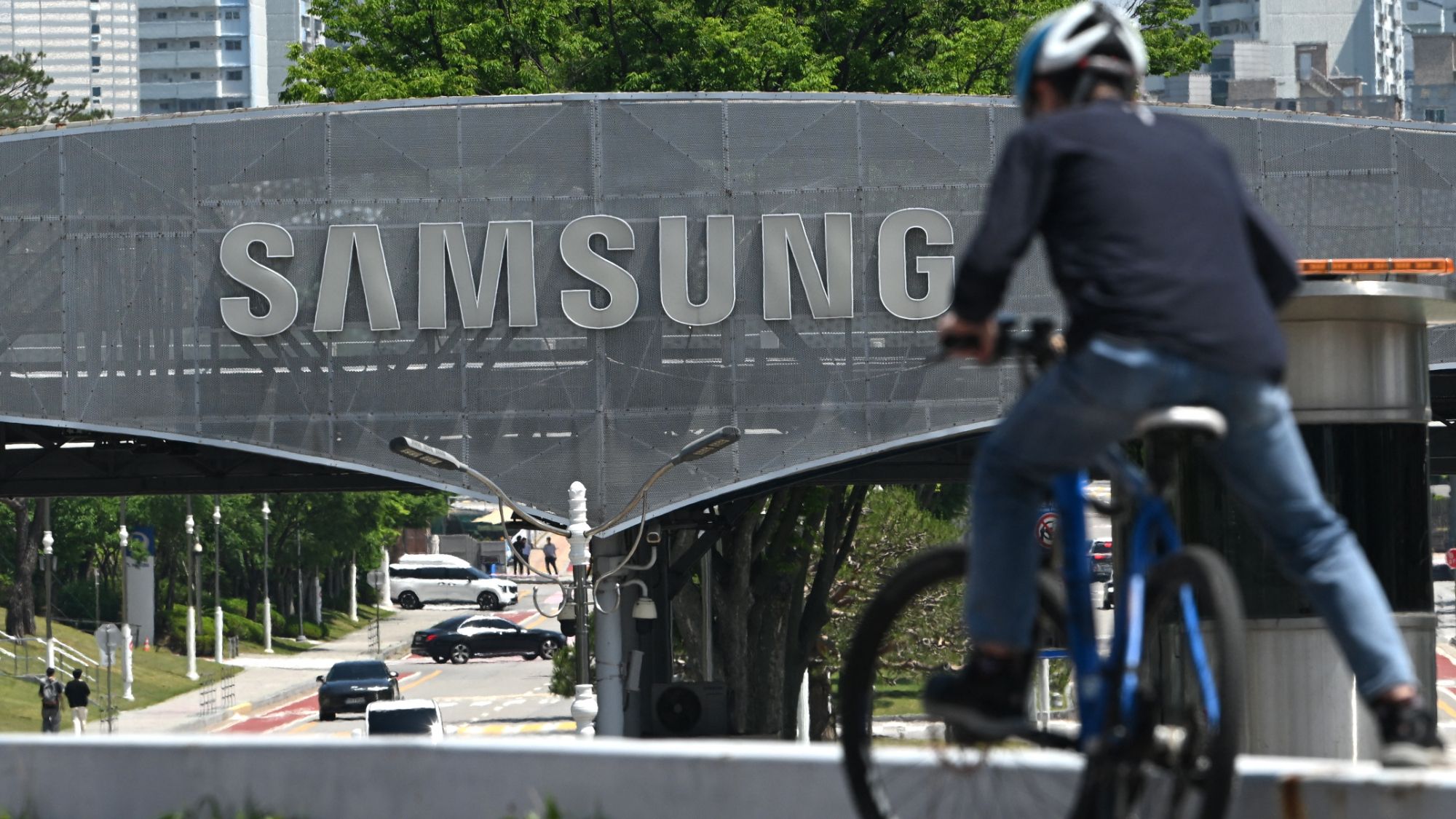
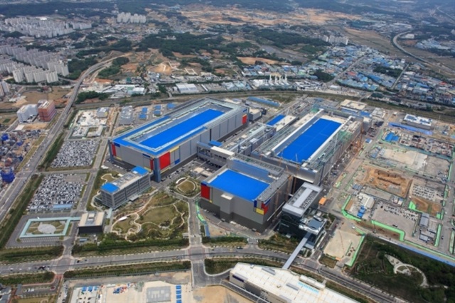
This isn’t just about adding another bullet point to a trade agreement. Silicon photonics is the real deal. It’s about moving data using light instead of electrons. Think faster, think more efficient. It’s the kind of tech that makes you wonder why we’re still fiddling with copper wires from the last century for certain applications. The current chatter suggests that Samsung, ever the opportunist, sees an opening. They’re nudging their way into this SiPh arena, and naturally, the Dutch — with their own R&D muscle and a history of being, well, Dutch about precision engineering — are invited to the party.
Beyond the EUV Tango
For years, the narrative has been dominated by ASML. Their EUV machines are the crown jewels, the gatekeepers to bleeding-edge chip manufacturing. And yes, South Korea needs those machines like a gambler needs a lucky streak. But relying solely on lithography suppliers, however dominant, is a precarious strategy. Diversification is the name of the game, and silicon photonics offers a whole new ball park. It’s a different kind of complexity, a different set of manufacturing challenges, and frankly, a different kind of opportunity.
The real kicker? This push aligns perfectly with the global AI gold rush. As models get bigger, stupider, and more insatiable, the infrastructure supporting them has to evolve at a breakneck pace. Traditional electrical interconnects are hitting their thermal and bandwidth limits. Silicon photonics promises to shatter those ceilings, allowing for faster communication between chips and within data centers. Samsung, with its vast manufacturing capabilities and its own AI ambitions, can’t afford to be left behind.
“We are exploring ways to enhance the bandwidth and energy efficiency of data transmission, which is becoming increasingly critical for AI workloads.” This quote, from some anonymous Samsung spokesperson trying to sound important, is the actual truth. Everything else is just corporate fluff.
Why Does This Matter for South Korea and the Netherlands?
For South Korea, it’s a chance to solidify its position not just as a chip maker, but as a chip innovator. Moving into SiPh means less reliance on others for the absolute cutting edge. It’s a strategic hedge. For the Netherlands, it’s a continuation of their high-tech prowess, particularly in optics and photonics research. They’ve got the brains; Samsung has the brawn (and the manufacturing scale). It’s a symbiosis that could actually work.
Of course, it won’t be easy. Silicon photonics manufacturing isn’t as mature as traditional CMOS. Integrating light-based components with electronic ones is a devilishly tricky business. Expect teething problems. Expect expensive prototypes. Expect more hand-wringing from analysts. But the alternative? Stagnation. And in the semiconductor world, stagnation is a one-way ticket to obsolescence. Samsung knows this. The Dutch know this. The question is, can they translate this potential into tangible progress, or will it just be another footnote in the ever-growing saga of semiconductor geopolitics?
Look, this isn’t about replacing ASML. That’s a fantasy. It’s about building a more resilient, more advanced semiconductor ecosystem. It’s about Samsung making a smart bet on the future, and the Netherlands getting a seat at that increasingly important table. The era of silicon is slowly, but surely, making way for the era of photonics. And those who don’t adapt will be left in the dark – literally.
What’s the Big Deal with Silicon Photonics, Anyway?
At its core, silicon photonics replaces electrical signals with optical signals (light) for data transmission. Imagine tiny lasers and light-sensitive components etched onto silicon wafers, much like traditional chips. This allows for significantly higher bandwidth (more data flow) and lower power consumption compared to electrical interconnects. Think of it as upgrading from a narrow country road to a multi-lane superhighway for your data. The AI boom is pushing data centers to their limits, and SiPh is seen as a key technology to overcome these bottlenecks.
Will This Partnership Actually Yield Results?
That’s the million-dollar question, isn’t it? Partnerships between nations and corporations are a mixed bag. They can accelerate innovation, or they can bog down in bureaucracy and competing interests. Samsung has a proven track record of pushing into new manufacturing frontiers, but SiPh is a more nascent field. The Netherlands brings critical R&D expertise. If they can find a smooth integration pathway, leveraging Samsung’s scale for mass production, then yes, it could yield significant results. But history is littered with promising collaborations that fizzled out. We’re cautiously optimistic, but with a healthy dose of skepticism. This isn’t a done deal, it’s a gamble.
How Does This Affect Existing Chip Manufacturing?
Silicon photonics doesn’t aim to replace traditional chip manufacturing entirely, but rather to complement and enhance it. It’s particularly relevant for the communication aspects of computing – moving data between processors, memory, and storage. So, while your CPU might still be built using EUV lithography for its core logic, the pathways connecting it to other components could be based on silicon photonics. This could lead to new types of chip architectures and advanced packaging solutions that integrate both electronic and photonic components. It’s an evolution, not an outright revolution of existing processes, but a significant one nonetheless.