Everyone’s been so focused on the bleeding edge of process nodes—the 3nm, the 2nm, the race to cram more transistors onto a single sliver of silicon. It’s been the narrative for years, the headline grabber, the ultimate arbiter of semiconductor supremacy. But what if the real innovation isn’t just about making those slivers smaller, but about how we connect them, how we stack them, how we coax maximum performance out of existing silicon? Intel’s recent moves, particularly their commitment to the Rio Rancho fab in New Mexico, suggest this very paradigm shift is underway.
And it’s a seismic one. For so long, the foundry game was about who could deliver the most advanced process node. TSMC has dominated this space, largely leaving Intel to play catch-up on its own manufacturing side. But Intel is now signaling a strategic pivot, a deliberate broadening of its foundry strategy that places significant emphasis on advanced packaging and, crucially, glass substrate technologies. Rio Rancho isn’t just another factory; it’s being groomed as a global nexus for this next generation of chip interconnects.
Why the Packaging Pivot? The AI Imperative
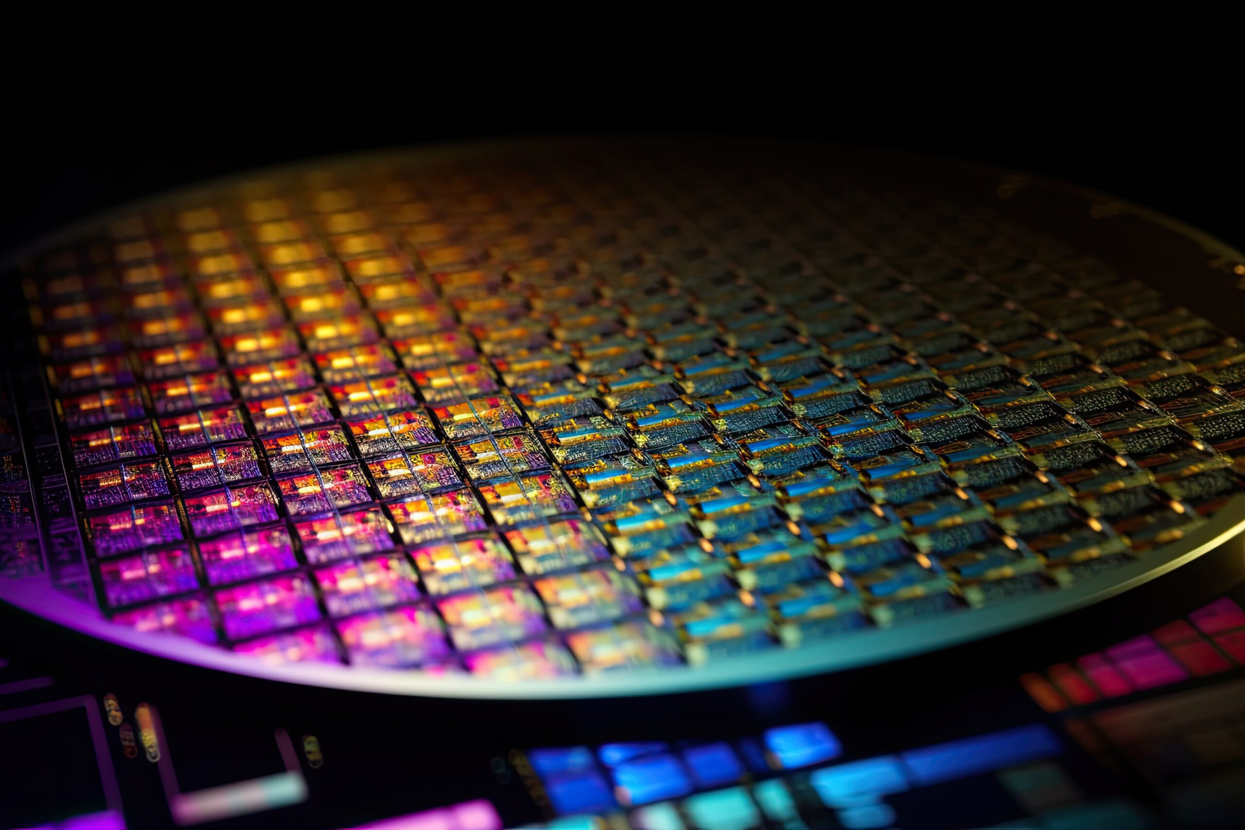
So, why the sudden spotlight on packaging? Look at the demands of modern AI. These workloads aren’t just about raw compute power from a single, monolithic chip. They’re about moving massive amounts of data between specialized processors—CPUs, GPUs, NPUs, and memory. Think of it as a super-highway system for data. A cutting-edge process node might build the fastest cars, but without an efficient network of roads, interchanges, and traffic management, those cars will just sit in gridlock. Advanced packaging is that network. It’s the complex architecture that allows different silicon dies, optimized for specific tasks, to work together in concert, often within a single module.
Intel’s announcement positions Rio Rancho as a key player in this ecosystem. They’re not just talking about slapping chips together; they’re talking about fabricating them with glass substrates, a notoriously difficult but potentially game-changing material. Glass substrates promise superior thermal management, higher density interconnects, and reduced signal loss compared to traditional organic substrates. This is critical for high-performance computing and AI, where heat is the enemy and every nanosecond of signal delay counts. This isn’t incremental improvement; it’s a fundamental architectural choice.
The strategy is to use Intel’s manufacturing prowess and global scale to be the partner of choice for customers seeking cutting-edge packaging solutions.
This quote, buried in the corporate speak, is the real story. Intel sees an opportunity not just to serve its own product lines but to become the go-to foundry for other companies that need sophisticated packaging. This is a direct challenge to the existing packaging leaders, many of whom are focused on specific niches or have their own internal supply chains. Intel, with its vast manufacturing footprint and now this explicit focus on packaging as a service, is aiming for broad market appeal.
The Architecture of Interconnects
At the heart of this lies a fundamental shift in how we design and manufacture semiconductors. For decades, the focus has been on monolithic integration – putting everything on one massive chip. But as we push the boundaries of physics and economics, this approach becomes increasingly challenging and expensive. Advanced packaging, often referred to as Chiplets, allows for a modular approach. You can design smaller, specialized dies (chiplets) and then assemble them using advanced packaging techniques like 2.5D or 3D stacking.
Intel’s Foveros technology, for example, enables 3D stacking, allowing logic, memory, and I/O dies to be integrated vertically. This significantly reduces the physical distance data needs to travel, leading to lower latency and higher bandwidth. Now, layering glass substrates onto this capability opens up even more performance ceilings. It’s like upgrading from a two-lane road to a multi-level, high-speed maglev system for your data.
But here’s the human element, the skepticism Chip Beat thrives on: Is this a genuine strategic pivot, or a clever reframing of a necessity? Intel has faced significant challenges in maintaining its lead in leading-edge process nodes. By emphasizing advanced packaging, they’re shifting the battlefield to an area where they can potentially use their existing strengths and extensive manufacturing capacity. It’s a smart move, certainly, but it also smacks of adapting to a market reality where monolithic perfection is becoming an increasingly elusive and costly dream.
Rio Rancho: The Test Case for a New Era
The choice of Rio Rancho for this ambitious endeavor is significant. It’s not a brand-new greenfield site; it’s an established Intel campus with a long history of advanced manufacturing. This suggests Intel isn’t just building a shiny new toy; they’re integrating this new capability into their existing operational muscle. This integration is key. For customers to trust Intel as a packaging partner, they need to see reliability, scalability, and a deep understanding of the manufacturing process, all of which are typically honed over years at established sites.
This also has implications for the broader semiconductor supply chain. As AI workloads grow exponentially, the demand for advanced packaging solutions will only skyrocket. Companies that can offer high-volume, high-quality advanced packaging will be in a prime position. Intel, with its global reach and newfound focus, is clearly signaling its intent to be a major player. This could reshuffle the deck, bringing more competition and potentially driving down costs for these critical technologies.
But the road ahead for glass substrates is paved with difficulty. Manufacturing them at scale, with the precision required for semiconductor interconnects, is an engineering Everest. If Intel can truly master this, Rio Rancho will indeed become a monument to a new era of chip design, one where the symphony of interconnects is as vital as the individual virtuosos on the silicon stage. If not, it becomes another chapter in the ongoing story of ambition meeting the harsh realities of semiconductor manufacturing.
**
🧬 Related Insights
- Read more: Apple’s Billion-Dollar App Store Crackdown: Greed or Grit?
- Read more: SK hynix’s Ethics Double: From Korean Trailblazer to Global Standard-Setter
Frequently Asked Questions**
What does Intel’s advanced packaging strategy mean for AI? Advanced packaging allows specialized chips (like CPUs and GPUs) to work together more efficiently within a single module, crucial for the massive data flow and complex computations required by AI.
Will this make Intel chips faster? Potentially, yes. By optimizing how different components communicate, advanced packaging can reduce latency and increase bandwidth, leading to overall performance improvements, especially for demanding workloads like AI.
Is Intel falling behind in process node technology? Intel has faced challenges in recent years keeping pace with leading competitors in the most advanced process nodes. Their focus on advanced packaging is seen as a strategic move to use other manufacturing strengths and offer competitive solutions.